Explain the construction and working of MOSFET
MOSFET

In case of JFET, the gate must be reverse biased for proper operation of the device i.e. it can only have negative gate operation for n-channel and positive gate operation for p-channel. That means we can only decrease the width of the channel from its zero-bias size. This type of operation is known as depletion-mode operation. Therefore, a JFET can only be operated in the depletion mode.
However, there is a field effect transistor that can be operated to enhance the width of the channel i.e. it can have enhancement-mode operation. Such a FET is called MOSFET.
Types of MOSFETs
There are two basic types of MOSFETs such as:
- Depletion-type MOSFET or D-MOSFET: The D-MOSFET can be operated in both depletion mode and the enhancement mode. For this reason it is also called depletion/enhancement MOSFET.
- Enhancement-type MOSFET or E-MOSFET: The E-MOSFET can be operated only in enhancement mode.
D-MOSFET
Fig.1 shows the constructional detail of n-channel D-MOSFET.

Fig.1 (n-Channel D-MOSFET)
The n-channel D-MOSFET is a piece of n-type material with a p-type region called substrate on the right and an insulated gate on the left as shown in fig.1.
The free electrons flowing from source to drain must pass through the narrow channel between the gate and the p-type region (i.e. substrate).
The gate construction of D-MOSFET is explained as below:
A thin layer of metal oxide, usually silicon dioxide (SiO2) is deposited over a small portion of the channel. A metallic gate is deposited over the oxide layer.
As SiO2 is an insulator, therefore, gate is insulated from the channel.
The substrate is connected to the source internally so that a MOSFET has three terminals such as Source (S), Gate (G) and Drain(D).
Since the gate is insulated from the channel, we can apply either negative or positive voltage to the gate. Therefore, D-MOSFET can be operated in both depletion-mode and enhancement-mode.
Symbols for D-MOSFET
There are two types of D-MOSFETs such as :
- n-channel D-MOSFET
- p-channel D-MOSFET
n-channel D-MOSFET
Fig.2 (i)shows the various parts of n-channel D-MOSFET.

Fig.2 (i)
The p-type substrate constricts the channel between the source and drain so that only a small passage remains at the left side.
Electrons flowing from source (when drain is positive w.r.t. source) must pass through this narrow channel.
The symbol for n-channel D-MOSFET is shown in fig.2 (ii).

Fig.2(ii)
The gate appears like a capacitor plate. Just to the right of the gate is a thick vertical line representing the channel.
The drain lead comes out of the top of the channel and the source lead connects to the bottom.
The arrow is on the substrate and points to the n-material, therefore we have nchannel D-MOSFET.
The substrate is connected to the source as shown in fig.2 (iii). This gives rise to a three terminal device.
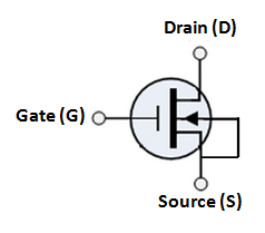
Fig.2 (iii)
p-channel D-MOSFET
Fig.3 (i) shows the various parts of p-channel D-MOSFET.

Fig.3 (i)
The n-type substrate constricts the channel between the source and drain so that only a small passage remains at the left side. The conduction takes place by the flow of holes from source to drain through this narrow channel.
The symbol for p-channel D-MOSFET is shown in fig.3 (ii).

Fig.3(ii)
The source is connected to substrate internally as shown in fig.3 (iii). This results in a three-terminal device.
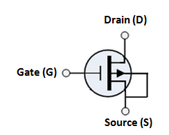
Fig.3(iii)
Circuit Operation of D-MOSFET
Fig.4 (i) shows the circuit of n-channel D-MOSFET.

Fig.4 (i)
The gate forms a small capacitor. One plate of this capacitor is the gate and the other plate is the channel with metal oxide layer as the dielectric.
When gate voltage is changed, the electric field of the capacitor changes which in turn changes the resistance of the n-channel.
Since the gate is insulated from the channel, we can apply either negative or positive voltage to the gate.
The negative gate operation is called depletion mode and positive gate operation is called enhancement mode.
-
Depletion mode:
Fig.5 (i) shows depletion mode operation of n-channel D-MOSFET.

Fig.5 (i) Fig.5 (ii)
Since gate is negative, it means electrons are on the gate as shown in fig.5 (ii).
These electrons repel the free electrons in the n-channel, leaving a layer of positive ions in a part of the channel as shown in fig.5 (ii).In other words, the n-channel is depleted of some of its free electrons.
Therefore, lesser number of free electrons are available for current conduction through the n-channel. This is same as increasing the channel resistance.
The greater the negative voltage on the gate, the lesser is the current from source to drain.
Thus by changing the negative voltage on the gate, we can vary the resistance of the n-channel and hence the current from source to drain.
As the action with negative gate depends upon depleting the channel of free electrons, the negative-gate operation is called depletion mode.
2. Enhancement mode:
Fig.6 (i) shows enhancement mode operation of n-channel D-MOSFET.

Fig.6 (i) Fig.6 (ii)
Again the gate acts like a capacitor. Since the gate is positive, it induces negative charges in the n-channel as shown in fig.6 (ii).
These negative charges are the free electrons drawn into the channel.
Because these free electrons are added to those already in the channel, the total number of free electrons in the channel is increased.
Thus a positive gate voltage enhances or increases the conductivity of the channel.
The greater the positive voltage on the gate, greater the conduction from source to drain.
Thus by changing the positive voltage on the gate, we can change the conductivity of the channel.
Because the action with a positive gate depends upon enhancing the conductivity of the channel, the positive gate operation is called enhancement mode.
The following points may be noted about D-MOSFET operation:
- In a D-MOSFET, the source to drain current is controlled by the electric field of capacitor formed at the gate.
- The gate of a D-MOSFET acts like a capacitor. For this reason it is possible to operate D-MOSFET with positive or negative gate voltage.
- As the gate of D-MOSFET forms a capacitor, therefore, negligible gate current flows whether positive or negative voltage is applied to the gate. For this reason, the input impedance of D-MOSFET is very high ranging from 10,000 MΩ to 10,000,00 MΩ.
- The extremely small dimensions of oxide layer under the gate terminal results is a very low capacitance and the D-MOSFET has, therefore, a very low input capacitance. This characteristics makes the D-MOSFET useful in high frequency applications.
E-MOSFET
Fig.7 shows the constructional details of n-channel E-MOSFET.

Fig.7
Its gate construction is similar to that of D-MOSFET.
The E-MOSFET has no channel between source and drain. The substrate extends completely to the SiO2 layer so that no channel exists.
The E-MOSFET requires a proper gate voltage to form a channel , called induced channel between the source and the drain.
It operates only in the enhancement mode and has no depletion mode.
Only by applying VGS of proper magnitude and polarity, the device starts conducting.
The minimum value of VGS of proper polarity that turns on the E-MOSFET is called threshold voltage [VGS(th)].
The n-channel device requires positive VGS (≥VGS(th)) and the p-channel device requires negative VGS(≥VGS(th)).
Symbols for E-MOSFET
Fig.8 (i) shows the schematic symbols for n-channel E-MOSFET and Fig.8 (ii) shows the schematic symbol for p-channel E-MOSFET.

Fig.8 (i) Fig.8 (ii)
Circuit Operation of E-MOSFET
Fig.9 (i) shows the circuit of n-channel E-MOSFE. The circuit action is as under:

Fig.9 (i)
(i) When VGS= 0V, as shown in fig.9 (i), there is no channel connecting source and drain.
The p-substrate has only a few thermally produced free electrons(minority carriers) so that drain current is almost zero. For this reason, E-MOSFET is normally OFF when VGS = 0V.
(ii) When VGS is positive, i.e gate is made positive as shown in fig.9(ii), it attracts free electrons into the p region. The free electrons combine with the holes next to the SiO2 layer.
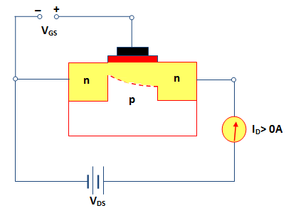
Fig.9 (ii)
If VGS is positive enough, all the holes touching the SiO2 layer are filled and free electrons begin to flow from the source to drain.
The effect is same as creating a thin layer of n-type material i.e. inducing a thin n-layer adjacent to the SiO2 layer.
Thus the E-MOSFET is turned ON and drain current ID starts flowing from the source to the drain.
The minimum value of VGS that turns the E-MOSFET ON is called threshold voltage[VGS(th)].
(iii) When VGS is less than VGS(th), there is no induced channel and the drain current IDis zero.
When VGS is equal to VGS(th), the E-MOSFET is turned ON and the induced channel conducts drain current from the source to the drain.
Beyond VGS(th), if the value of VGS is increased,the newly formed channel becomes wider, causing to ID to increase.
If the value of VGS decreases not less than VGS(th), the channel becomes narrower and ID will decrease.
You Might Like The Following Articles
- What is a Transistor ? Describe the Transistor Action in Detail . Explain the Operation of Transistor as an Amplifier
- Explain the construction and working of a JFET. What is the difference between a JFET and a BJT
- Describe the output Characteristics and transfer characteristics of JFET . Explain different methods of biasing of a JFET
- Explain the construction and working of MOSFET
- Unijunction Transistor
- Discuss the essentials of a transistor Oscillator . Explain the action of tuned collector oscillator , Colpitt’s oscillator and Hartley oscillator