Fabrication of Components on Monolithic IC
Fabrication of Components on Monolithic IC

The outstanding feature of an IC is that is comprises an number of circuit elements inseparably associated in a single small package to perform a complete electronic circuit. We shall now see how various circuit elements (such as transistors, diodes, resistors etc.) can be fabricated in an IC form.
Diodes and Transistors
Diodes and transistors are usually formed using the epitaxial planar diffusion process described previous article.
Diodes
One or more diodes are formed by diffusing one or more small n-type deposits at appropriate locations on the substrate.
Fig. 1 shows how a diode is formed on a portion of substrate of a monolithic IC.
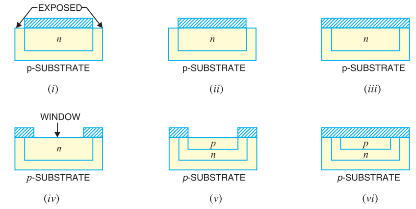
Fig 1
Part of SiO2 layer is etched off, exposing the epitaxial layer as shown in Fig. 1 (i).
The wafer is then put into a furnace and trivalent atoms are diffused into the epitaxial layer.
The trivalent atoms change the exposed epitaxial layer from n-type semi-conductor to p-type.
Thus we get an island of n-type material under the SiO2 layer as shown in Fig. 1 (ii).
Next pure oxygen is passed over the wafer to form a complete SiO2 layer as shown in Fig. 1 (iii).
A hole is then etched at the centre of this layer ; thus exposing the n-epitaxial layer [See Fig. 1 (iv)].This hole in SiO2 layer is called a window.
Now we pass trivalent atoms through the window.
The trivalent atoms diffuse into the epitaxial layer to form an island of p-type material as shown in Fig. 1 (v).
The SiO2 layer is again formed on the wafer by blowing pure oxygen over the wafer [See Fig. 1 (vi)].
Thus a p-n junction diode is formed on the substrate .
The last step is to attach the terminals. For this purpose, we etch the SiO2 layer at the desired locations as shown in Fig 2 (i).

Fig 2
By depositing metal at these locations, we make electrical contact with the anode and cathode of the integrated diode. Fig. 2 (ii) shows the electrical circuit of the diode .
Transistor
Transistors are formed by using the same principle as for diodes. Fig. 3 shows how a transistor is formed on a portion of the substrate of a monolithic IC. For this purpose, the steps used for fabricating the diode are carried out upto the point where p island has been formed and sealed off [See Fig. 1 (vi) above]. This Fig. is repeated as Fig. 3 (i) and shall be taken as the starting point in order to avoid repetition.
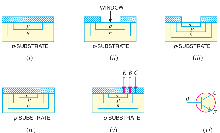
Fig 3
A window is now formed at the centre of SiO2 layer, thus exposing the p-epitaxial layer as shown in Fig. 3 (ii).
Then we pass pentavalent atoms through the window. The pentavalent atoms diffuse into the epitaxial layer to form an island of n-type material as shown in Fig. 3 (iii).
The SiO2 layer is re-formed over the wafer by passing pure oxygen [See Fig. 3 (iv)].
The terminals are processed by etching the SiO2 layer at appropriate locations and depositing the metal at these locations as shown in Fig. 3 (v). In this way, we get the integrated transistor.
Fig. 3 (vi) shows the electrical circuit of a transistor.
Resistors
Fig. 4 shows how a resistor is formed on a portion of the substrate of a monolithic IC.

Fig 4
For this purpose, the steps used for fabricating diode are carried out upto the point where n island has been formed and sealed off [Refer back to Fig. 1 (iii)].
This figure is repeated as Fig. 4 (i) and shall be taken as the starting point in order to avoid repetition.
A window is now formed at the centre of SiO2 layer, thus exposing the n-epitaxial layer as shown in Fig. 4 (ii). Then we diffuse a p-type material into the n-type area as shown in Fig. 4 (iii).
The SiO2 layer is re-formed over the wafer by passing pure oxygen [See Fig. 4 (iv)].
The terminals are processed by etching SiO2 layer at two points above the p island and depositing the metal at these locations [See Fig. 4 (v)].
In this way, we get an integrated resistor. Fig. 4 (vi) shows the electrical circuit of a resistor.
The value of resistor is determined by the material, its length and area of cross-section. The high-resistance resistors are long and narrow while low-resistance resistors are short and of greater cross-section.
Capacitors
Fig. 5 shows the process of fabricating a capacitor in the monolithic IC.

Fig 5
The first step is to diffuse an n-type material into the substrate which forms one plate of the capacitor as shown in Fig. 5 (i).
Then SiO2 layer is re-formed over the wafer by passing pure oxygen as shown in Fig. 1 (ii).
The SiO2 layer formed acts as the dielectric of the capacitor.
The oxide layer is etched and terminal 1 is added as shown in Fig. 5 (iii).
Next a large (compared to the electrode at terminal 1) metallic electrode is deposited on the SiO2 layer and forms the second plate of the capacitor.
The oxide layer is etched and terminal 2 is added. This gives an integrated capacitor.
The value of capacitor formed depends upon the dielectric constant of SiO2 layer, thickness of SiO2 layer and the area of cross-section of the smaller of the two electrodes.