Combinational MOS Logic Circuits
Last Updated on November 28, 2016 by Sasmita
Combinational logic circuits or gates are the basic building blocks of all digital systems.
These circuits or gates perform Boolean operations on multiple input variables and determine the outputs as Boolean functions of the inputs.
We will discuss simple circuit configurations such as two-input NAND and NOR gates and then expand our analysis to more general cases of multiple-input circuit structures.
In its most general form, a combinational logic circuit, or gate, performing a Boolean function can be represented as a multiple-input, single-output system, as shown in the figure below.

Figure 1: Combinational Logic Circuit
Node voltages, referenced to the ground potential, represent all input variables.
Using positive logic convention, the Boolean (or logic) value of “1” can be represented by a high voltage of VDD, and the Boolean (or logic) value of “0” can be represented by a low voltage of 0.
The output node is loaded with a capacitance Cload, which represents the combined capacitances of the parasitic device in the circuit.
Static and Dynamic CMOS Design
In static CMOS circuit style, each gate output is connected to either VDD or VSS via a low-resistance path,at every point in time (except during the switching transients),
Also, the outputs of the gates assume at all times the value of the Boolean function implemented by the circuit (ignoring, once again, the transient effects during switching periods).
Whereas in dynamic circuit class, that relies on temporary storage of signal values on the capacitance of high-impedance circuit nodes.
The dynamic approach has the advantage that the resulting gate is simpler and faster. On the other hand, its design and operation are more involved than those of its static counterpart, due to an increased sensitivity to noise.
Complementary CMOS
A static CMOS gate is a combination of two networks, called the pull-up network (PUN) and the pull-down network (PDN) as shown in figure below.
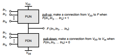
Figure 2: Complementary logic gate as a combination of a PUN (pull-up network) and a PDN (pull-down network).
The figure shows a generic N input logic gate where all inputs are distributed to both the pull-up and pull-down networks.
The function of the PUN is to provide a connection between the output and VDD anytime the output of the logic gate is meant to be 1 (based on the inputs).
Similarly, the function of the PDN is to connect the output to VSS when the output of the logic gate is meant to be 0.
The PUN and PDN networks are constructed in a mutually exclusive fashion such that one and only one of the networks is conducting in steady state.
In constructing the PDN and PUN networks, the following observations should be kept in mind:
- A transistor can be thought of as a switch controlled by its gate signal. An NMOS switch is on when the controlling signal is high and is off when the controlling signal is low. A PMOS transistor acts as an inverse switch that is on when the controlling signal is low and off when the controlling signal is high.
- The PDN is constructed using NMOS devices, while PMOS transistors are used in the PUN. The primary reason for this choice is that NMOS transistors produce “strong zeros,” and PMOS devices generate “strong ones”.
- To illustrate this, consider the examples shown in Figure 3. In Figure 3(a), the output capacitance is initially charged to VDD. Two possible discharge scenario’s are shown. An NMOS device pulls the output all the way down to GND, while a PMOS lowers the output no further than |VTp| — the PMOS turns off at that point, and stops contributing discharge current. NMOS transistors are hence the preferred devices in the PDN.
- Similarly, two alternative approaches to charging up a capacitor are shown in Figure 3(b), with the output load initially at GND. A PMOS switch succeeds in charging the output all the way to VDD, while the NMOS device fails to raise the output above VDD-VTn. This explains why PMOS transistors are preferentially used in a PUN.
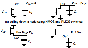
Figure 3 : examples illustrate why an NMOS should be used as a pulldown transistor, while a PMOS should be used as a pull-up device.
- A set of construction rules can be derived to construct logic functions . For example:NMOS devices connected in series corresponds to an AND function. With all the inputs high, the series combination conducts and the value at one end of the chain is transfered to the other end.
- Similarly, NMOS transistors connected in parallel represent an OR function. A conducting path exists between the output and input terminal if at least one of the inpurs is high.
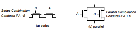
Figure 4 : NMOS logic rules — series devices implement an AND, and parallel devices implement an OR.
- Using similar arguments, construction rules for PMOS networks can be formulated. A series connection of PMOS conducts if both inputs are low, representing a NOR function , while PMOS transistors in parallel implement a NAND .
- Using De Morgan’s theorems:
![]()
and ![]()
it can be shown that the pull-up and pull-down networks of a complementary CMOS structure are dual networks.
- This means that a parallel connection of transistors in the pull-up network corresponds to a series connection of the corresponding devices in the pull-down network, and vice versa.
- Therefore, to construct a CMOS gate, one of the networks (e.g., PDN) is implemented using combinations of series and parallel devices.
- The other network (i.e., PUN) is obtained using duality principle by , replacing series subnets with parallel subnets, and parallel subnets with series subnets.
- The complete CMOS gate is constructed by combining the PDN with the PUN.
- The complementary gate is naturally inverting, implementing only functions such as NAND, NOR, and XNOR. The realization of a non-inverting Boolean function (such as AND OR, or XOR) in a single stage is not possible, and requires the addition of an extra inverter stage.
- The number of transistors required to implement an N-input logic gate is 2N.
Two input NAND Gate
Figure 4 shows a two-input NAND gate:
![]()

Figure 4 :Two-input NAND gate in complementary static CMOS style
The PDN network consists of two NMOS devices in series that conduct when both A and B are high.
The PUN is the dual network, and consists of two parallel PMOS transistors.
This means that F is 1 if A = 0 or B = 0, which is equivalent to

The truth table for the simple two input NAND gate is given in Table 1.

Table 1 :Truth Table for 2 input NAND
It can be verified that the output F is always connected to either VDD or GND, but never to both at the same time.