Demodulation of FM Waves
Last Updated on June 11, 2020 by Sasmita
Demodulation of FM Waves
The demodulation process of FM waves is exactly opposite to that of the frequency modulation. After demodulation, we get the original modulating signal at the demodulation output.
FM demodulator or detector is basically a frequency to amplitude converter. It is expected to convert the frequency variations in FM wave at its input into amplitude variations at its output to recover the original modulating signal.
Requirements of FM Demodulator (Detector)
The FM demodulator must satisfy the following requirements:
(i) It must convert frequency variations into amplitude variations.
(ii) This conversion must be linear and efficient.
(iii) The demodulator circuit should be insensitive to amplitude changes. It should respond only to the frequency changes.
(iv) It should not be too critical in its adjustment and operation.
Classification of FM Demodulators
Figure.1 shows the classification of FM Demodulators.
Fig.1: Classification of FM Demodulators
Balanced Frequency Discriminator
The frequency discriminator operates on the principle of the slope detection.
Principle of Slope Detection
Let us consider a tuned circuit as shown in figure 1.
Fig. 1: Tuned Circuit
A frequency modulated signal is applied at the input of this tuned circuit.
The center frequency of the FM signal is fc and the frequency deviation is Δf.
The resonant frequency of the tuned circuit is deliberately adjusted to (fc + Δf) as shown in figure 1.
As depicted in figure 1, the amplitude of the output voltage of the tank circuit depends on the frequency deviation of the input FM signal.
Simple Slope Detector ( Frequency Discriminator )
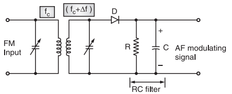
The circuit diagram of a simple slope detector is as shown in figure 2.
Fig.2 : Simple Slope Detector
The output voltage of the tank circuit is then applied to a simple diode detector of an RC load with proper time constant.
This detector is identical to the AM diode detector. Even though the slope detector circuit is simple it has the following drawbacks.
Drawbacks of Slope Detector
(i) It is inefficient.
(ii) It is linear only over a limited frequency range.
(iii) It is difficult to adjust as the primary and secondary winding of the transformer must be tuned to slightly different frequencies.
Advantages of Slope Detector
The only advantages of the basic slope detector circuit is its simplicity.
To overcome the drawbacks of the simple slope detector, a Balanced slope detector is used.
Balanced Slope Detector (Balanced Frequency Discriminator)
The circuit diagram of the balanced slope detector is shown in Figure. 3.
Fig.3 : Balanced Slope Detector
As shown in the circuit diagram, the balanced slope detector consists of two slope detector circuits.
The input transformer has a center tapped secondary. Hence, the input voltages to the two slope detectors are 180° out of phase.
There are three tuned circuits.
Out of them, the primary is tuned to IF i.e., fc .
The upper tuned circuit of the secondary (T1) is tuned above fc by Δf i.e., its resonant frequency is (fc+ Δf).
The lower tuned circuit of the secondary is tuned below fc by Δf i.e., at (fc – Δf).
R1C1 and R2C2 are the filters used to bypass the RF ripple.
Vo1 and Vo2 are the output voltages of the two slope detectors.
The final output voltage Vo is obtained by taking the subtraction of the individual output voltages, Vo1 and Vo2, i.e.,
Working Operation of the Circuit
The circuit operation can be explained by dividing the input frequency into three ranges as follows:
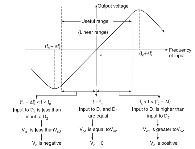
(i) fin = fc: When the input frequency is instantaneously equal to fc, the induced voltage in the T1 winding of secondary is exactly equal to that induced in the winding T2.
Thus, the input voltages to both the diodes D1 and D2 will be the same.
Therefore, their dc output voltages Vo1 and Vo2 will also be identical but they have opposite polarities. Hence, the net output voltage Vo = 0.
(ii) fc < fin < (fc + Δf): In this range of input frequency, the induced voltage in the winding T1 is higher than that induced in T2.
Therefore, the input to D1 is higher than D2.
Hence, the positive output Vo1 of D1 is higher than the negative output Vo2 of D2.
Therefore, the output voltage Vo is positive.
As the input frequency increases towards (fc + Δf), the positive output voltage increases as shown in 4.
Fig.4: Characteristics of the balanced slope detector
If the output frequency goes outside the range of (fc – Δf) to (fc + Δf), the output voltage will fall due to the reduction in tuned circuit response.
Advantages
(i) This circuit is more efficient than simple slope detector.
(ii) It has better linearity than the simple slope detector.
Drawbacks
(i) Even though linearity is good, it is not good enough.
(ii) This circuit is difficult to tune since the three tuned circuits are to be tuned at different frequencies i.e., fc, (fc+Δf) and (fc – Δf).
(iii) Amplitude limiting is not provided.
Zero Crossing Detector
The zero crossing detector operator on the principle that the instantaneous frequency of an FM wave is approximately given by,
where Δt is the time difference between the adjacent zero crossover points of the FM wave as shown in figure 5.
Fig.6
Let us consider a time-duration T as shown in figure 6.
The time T is chosen such that it satisfies the following two conditions:
(i) T should be small compared to (1/W) wheel, W is the bandwidth of the message signal.
(ii) T should be large as compared to (1/fc) where fc is the carrier frequency of the FM wave.
Let the number of zero crossings during interval T be denoted by n0. Hence, Δt i.e., the time between the adjacent zero crossing points is given by,
By definition of the instantaneous frequency, we know that there is a linear relation between fi and message signal x(t). Hence, we can recover x(t) if n0 is known. This can be achieved by using a zero crossing detector of figure 7.
Fig.7: Block Diagram of Zero Crossing Detector


