Explain Logic AND Gate and Its Operation with Truth Table
Last Updated on November 6, 2015 by Sasmita
AND Gate
The AND gate performs logical multiplication, more commonly known as AND function.
The AND gate has two or more inputs and a single output, as shown in the standard logic symbols in fig 1.
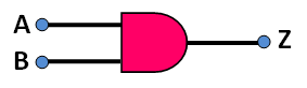
Fig. 1
The AND gate provides high output only when all inputs are high.
The fig.2 shows one way to build a 2-input AND gate using diodes.
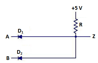
Fig. 2
The input voltages are labelled A and B, while the output voltage Z.
When voltages of both inputs are high, both the diodes are non-conducting because the diodes are reverse-biased. Since the diodes are off, no current flows through resistor R, and the output is pulled up to the supply voltage VCC (+5). Thus for both inputs high, output is high.
But when input voltage of either or both terminals are low, cathode(s) of the diode(s) connected to low input terminal(s) is/are grounded and the diode(s) become(s) forward-biased, resulting in flow of current through resistor R. So in such a condition, voltage of the output terminal becomes low.
Symbols used for AND gates with 2, 3 and N inputs are shown in fig 3 (a), (b) and (c) respectively.
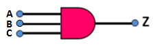
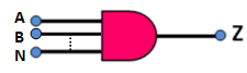
Fig 3 (a) Fig 3 (b) Fig 3 (c)
The input A, B, C….and N are logic voltage levels and output Z is a logic voltage level whose value is the result of the AND operation on A, B, C….and N.
The operation of the AND gate is such that the output is high or 1 if and only if all the inputs are high or 1. Mathematically it is written as :
Z = A AND B AND C …AND n = A.B.C…….n = ABC….n ….(1)
Where A, B, C…..N are input variables and Z is the output variable.
Truth Table of AND Gate
The logical operation of the 2-input and 3-input AND gate is described in truth table shown in table 1 and table 2 respectively .
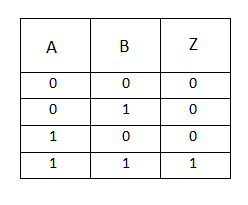
Table 1 : Truth table of 2 -input AND Gate

Table 2: Truth Table of 3-input AND Gate
The AND gate may be thought of as an electrical circuit in which the switches are connected in series. Lamp will glow (output will be present) only when all the switches are closed.
The basic purpose of an AND gate is thus to determine when certain conditions are simultaneously true, as indicated by high levels on all its inputs, and to produce a high on its output indicating this condition.
AND gate can be used to block or transmit data in digital systems. Let an AND gate shown in fig.4 be connected in an electronic circuit.
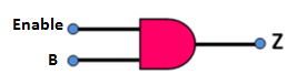
Fig. 4
If ENABLE input is low, the output Z will be low for each possible level of B. Thus, in this case the data from the input is blocked i.e. the data cannot be transmitted to the output. However, when ENABLE is made high, the output Z will follow the input at B i.e. if B is high , Z will be high and if B is low, Z will be low. In this case the data at input B is enabled to be transmitted to the output.
Transistor AND Gate
Fig. 5 depicts a transistor AND gate.
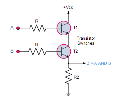
Fig 5
A simple 2-input logic AND gate can be constructed using RTL Resistor-transistor switches connected together as shown above with the inputs connected directly to the transistor bases.
In this case both transistors must be saturated “ON” for an output at Q.
Standard Package of AND Gate
Fig 6 depicts the pinout diagram of IC7408, a TTL quad-2 input AND gate.
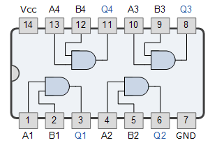
Fig. 6
This IC contains four 2-input AND gates. It is 14-pin DIP. After connecting a supply voltage of +5V to pin-14 and a ground to pin-7, we can connect one or more of the AND gates to the other TTL devices.
Pulsed Operation of AND Gate
Fig 7 shows two pulses A and B as inputs to an AND gate.
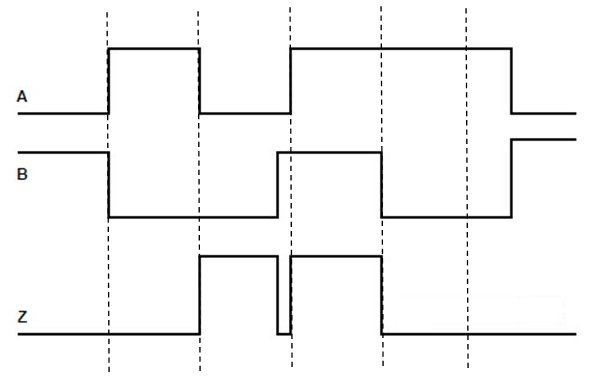
Fig.7
When either input is low the output is low. Only when both inputs are high, the output is high.