Explain the Logic NOT Gate or Inverter and its Operation with Truth Table
Last Updated on November 6, 2015 by Sasmita
NOT Gate or Inverter
The Not Gate (or inverter) performs a basic logic function called inversion or complementation. The purpose of the inverter is to change one logic level to the opposite level. In terms of bits, it changes a 1 to 0 and vice-versa.
This gate has only one input and one output. NOT gate is called the inverter because output state is always opposite to the input state, so when the input is low signal, output is high signal and vice-versa.
It is called NOT gate because the output state is always opposite to that of the input state. A transistor may be used as an inverter, as shown in fig 1.

Fig.1
When the input signal to the base of transistor, is zero, base current of transistor is zero, as no current flows in collector circuit and the output voltage remains equal to VCC i.e. 5V. On the other hand when the input signal is high, base current flows through the transistor resulting in flow of saturation current in collector circuit. Because of high collector current there will be large voltage drop across the collector resistance RC and so output Vout will be at low level.
Symbols used for representing inverters are shown in fig.2
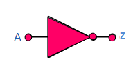
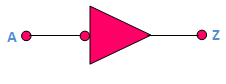
Fig 2 (a) Fig. 2(b)
Bubble shown in symbols, itself shows that output is a complement of input. The placement of the bubble on the input or output of a logic element is determined by the active state of the input signal (pulse or level). The active state is the state (1 or 0) when the signal is considered to be present on the output. When the active state of the input is a 0, the bubble is placed on the input.
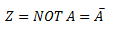
The logic equation of the NOT gate is written as
 Truth Table of NOT Gate
And is read as ‘Z equals NOT A’or ‘Z equals complement of A’. The truth table of a NOT gate is given in table 1
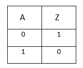
Table 1
Standard Package
It contains the TTL hex inverter. It is a 14-pin dual-in-line package. Fig 3 depicts the pinout diagram of IC 7404.
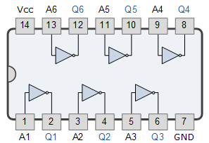
Fig 3
Pulsed Operation
Fig 4 depicts the output of an inverter (or NOT gate) for a pulse input.
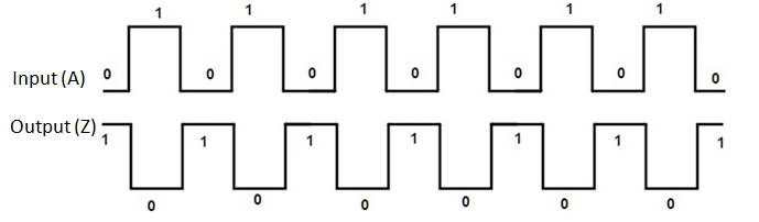
Fig.4
When the input is low, the output is high and when the input is high, the output is low. Thus the inverter produced inverted pulses.