Explain the Principle of Operation of MOS Inverter
Last Updated on November 18, 2016 by Sasmita
The inverter is truly the nucleus of all digital designs.
Once its operation and properties are clearly understood, designing more intricate structures such as NAND gates, adders, multipliers, and microprocessors is greatly simplified.
The analysis of inverters can be extended to explain the behavior of more complex gates such as NAND, NOR, or XOR, which in turn form the building blocks for modules such as multipliers and processors.
In this article, we will discuss the CMOS inverter. This is certainly the most popular at present and therefore deserves our special attention.
Principle of Operation
The logic symbol and truth table of ideal inverter is shown in figure given below.

Logic symbol

Truth Table
Here A is the input and B is the inverted output.
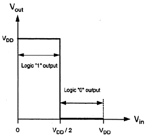
Using positive logic, the Boolean value of logic 1 is represented by VDD and logic 0 is represented by 0.
Vth is the inverter threshold voltage, which is equal to VDD /2, where VDD is the output voltage.
The output is switched from 0 to VDD when input is less than Vth.
So, for 0<Vin<Vth , output is equal to logic 0 input and for Vth<Vin< VDD ,output is equal to logic 1 input.
The generalized circuit of an nMOS inverter is shown in the figure below.

Generalized Circuit for an nMOS Inverter
From the above figure, we can see that the input voltage of the inverter is equal to the gate to source voltage of nMOS transistor and output voltage of inverter is equal to drain to source voltage of nMOS transistor.
The source to substrate voltage of nMOS is also called driver for transistor which is grounded; so VSS= 0.
The output node is connected with a lumped capacitance used for VTC (Voltage Transfer Characteristics).
Resistive Load Inverter
The basic structure of a resistive load inverter is shown in the figure below.
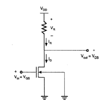
Resistive Load nMOS Inverter Circuit
Here, enhancement type nMOS acts as the driver transistor.
The load consists of a simple linear resistor RL.
The power supply of the circuit is VDD and the drain current ID is equal to the load current IR.
Circuit Operation
When the input of the driver transistor is less than threshold voltage Vth(Vin < Vth), the driver transistor is in the cut–off region and does not conduct any current.
So, the voltage drop across the load resistor is ZERO and output voltage is equal to the VDD.
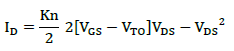
Now, when the input voltage increases further, driver transistor will start conducting the non-zero current and nMOS goes in saturation region.
Mathematically,
![]()
Increasing the input voltage further, driver transistor will enter into the linear region and output of the driver transistor decreases.
VTC of the resistive load inverter is shown below indicating the operating mode of driver transistor and voltage points.

Voltage Transfer Characteristic of Resistive Load Inverter
Inverter with n-type MOSFET Load
The main advantage of using MOSFET as load device is that the silicon area occupied by the transistor is smaller than the area occupied by the resistive load.
Here, MOSFET is an active load and inverter with active load gives a better performance than the inverter with resistive load.
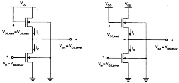
Enhancement Load NMOS
Two inverters with enhancement-type load device are shown in the figure.
(a) (b)
Fig. (a) Saturated Enhancement type nMOS type Load
(b) Linear Enhancement type nMOS type Load
Load transistor can be operated either, in saturation region or in linear region, depending on the bias voltage applied to its gate terminal.
The saturated enhancement load inverter is shown in the fig.(a).
It requires a single voltage supply and simple fabrication process and so VOH is limited to the VDD – VT.
The linear enhancement load inverter is shown in the fig. (b).
It always operates in linear region; so VOH level is equal to VDD .
Linear load inverter has higher noise margin compared to the saturated enhancement inverter.
But, the disadvantage of linear enhancement inverter is, it requires two separate power supply and both the circuits suffer from high power dissipation.
Therefore,enhancement inverters are not used in any large-scale digital applications.
Depletion Load NMOS
Drawbacks of the enhancement load inverter can be overcome by using depletion load inverter.
Compared to enhancement load inverter, depletion load inverter requires few more fabrication steps for channel implant to adjust the threshold voltage of load.
The advantages of the depletion load inverter are:
- sharp VTC transition
- better noise margin
- single power supply
- smaller overall layout area
Inverters with depletion-type load device are shown in the figure below.
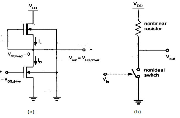
Fig : (a) Inverter Circuit with Depletion type nMOS load (b) Simplified Equivalent Circuit of nMOS Load
As shown in the figure, the gate and source terminal of load are connected; So, VGS = 0.
Thus, the threshold voltage of the load is negative. Hence,
VGS,Load > VT,Load, is satisfied
Therefore, load device always has a conduction channel regardless of the input and output voltage level.
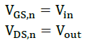
When the load transistor is in saturation region, the load current is given by,
When the load transistor is in linear region, the load current is given by,

The voltage transfer characteristics of the depletion load inverter is shown in the figure given below.

Typical VTC of Depletion Load nMOS Inverter
CMOS Inverter – Circuit, Operation and Description
The CMOS inverter circuit is shown in the figure.

CMOS Inverter Circuit
Here, nMOS and pMOS transistors work as driver transistors; when one transistor is ON, other is OFF.
This configuration is called complementary MOS (CMOS).
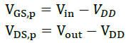
The input is connected to the gate terminal of both the transistors such that both can be driven directly with input voltages.
Substrate of the nMOS is connected to the ground and substrate of the pMOS is connected to the power supply,VDD.
So VSB = 0 for both the transistors.
And
When the input of nMOS is smaller than the threshold voltage (Vin < VTO,n), the nMOS is cut – off and pMOS is in linear region. So, the drain current of both the transistors is zero.
![]()
Therefore, the output voltage VOH is equal to the supply voltage.
![]()
When the input voltage is greater than the VDD+ VTO,p, the pMOS transistor is in the cut-off region and the nMOS is in the linear region, so the drain current of both the transistors is zero.
![]()
Therefore, the output voltage VOL is equal to zero.
![]()
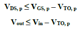
The nMOS operates in the saturation region if Vin > VTO , and if following conditions are satisfied.

The pMOS operates in the saturation region if Vin < VDD + VTO,p , and if following conditions are satisfied.
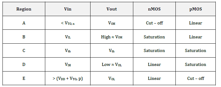
For different value of input voltages, the operating regions are listed below for both transistors.
The VTC of CMOS is shown in the figure below:

VTC of CMOS Inverter