Flip-Flops
Last Updated on September 27, 2015 by Sasmita
Flip-Flops
Flip-flops are the basic building blocks of sequential circuits and are used as basic element for storing information.
One flip-flop can store one bit of information.
Flip-flops belong to sequential circuit elements, whose output depends not only on the current inputs, but also on previous inputs and outputs.
Flip-flops, have their content change only either at the rising or falling edge of the enable signal. This enable signal is usually the controlling clock signal.
After the rising or falling edge of the clock, the flip-flop content remains constant even if the input changes.
There are basically four main types of flip-flops: SR, D, JK, and T.
S-R Flip Flop
The SET-RESET flip flop is designed with the help of either two NOR gates or two NAND gates. These flip flops are also called S-R Latch.
S-R Flip Flop using NOR Gate
The design of such a flip flop includes two inputs, called the SET [S] and RESET [R]. There are also two outputs, Q and Q’.
The diagram and truth table is shown below.

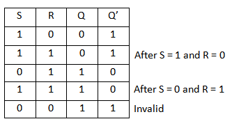
(a) Logic Diagram

(b) Truth Table
Fig.1 SR Flip-flop Using NOR gates
Operation
From the diagram it is evident that the flip flop has mainly four states. They are
S=1, R=0: Q=1, Q’=0
This state is also called the SET state.
S=0, R=1: Q=0, Q’=1
This state is known as the RESET state.
In both the states you can see that the outputs are just compliments of each other and that the value of Q follows the value of S.
S=0, R=0: Q & Q’ = Remember
If both the values of S and R are switched to 0, then the circuit remembers the value of S and R in their previous state.
S=1, R=1: Q=0, Q’=0 [Invalid]
This is an invalid state because the values of both Q and Q’ are 0. They are supposed to be compliments of each other. Normally, this state must be avoided.
S-R Flip Flop using NAND Gate
The circuit of the S-R flip flop using NAND Gate and its truth table is shown below.

(a) Logic Diagram
(b) Truth Table
Fig.2 SR Flip-flop Using Nand gates
Operation
Like the NOR Gate S-R flip flop, this one also has four states. They are
S=1, R=0 : Q=0, Q’=1
This state is also called the SET state.
S=0, R=1 : Q=1, Q’=0
This state is known as the RESET state.
In both the states you can see that the outputs are just compliments of each other and that the value of Q follows the compliment value of S.
S=0, R=0 : Q=1, & Q’ =1 [Invalid]
If both the values of S and R are switched to 0 it is an invalid state because the values of both Q and Q’ are 1. They are supposed to be compliments of each other. Normally, this state must be avoided.
S=1, R=1 : Q & Q’= Remember
If both the values of S and R are switched to 1, then the circuit remembers the value of S and R in their previous state.
Clocked S-R Flip Flop
It is also called a Gated S-R flip flop.
The problems with S-R flip flops using NOR and NAND gate is the invalid state. This problem can be overcome by using a bistable SR flip-flop that can change outputs when certain invalid states are met, regardless of the condition of either the Set or the Reset inputs.
For this, a clocked S-R flip flop is designed by adding two AND gates to a basic NOR Gate flip flop. The circuit diagram and truth table is shown below.
 (a) Logic Diagram
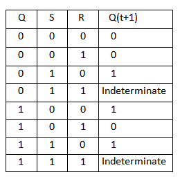
(b) Truth Table
Fig.3 Clocked SR Flipflop
Operation
A clock pulse [CP] is given to the inputs of the AND Gate.
When the value of the clock pulse is ‘0’, the outputs of both the AND Gates remain ‘0’.
As soon as a pulse is given the value of ‘1’ i.e CP turns ‘1’. This makes the values at S and R to pass through the NOR Gate flip flop.
But when the values of both S and R turn ‘1’, the HIGH value of CP causes both of them to turn to ‘0’ for a short moment.
As soon as the pulse is removed, the flip flop state becomes intermediate.
Thus either of the two states may be caused, and it depends on whether the set or reset input of the flip-flop remains a ‘1’ longer than the transition to ‘0’ at the end of the pulse.
Thus the invalid states can be eliminated.
D Flip Flop
The circuit diagram and truth table is given below.
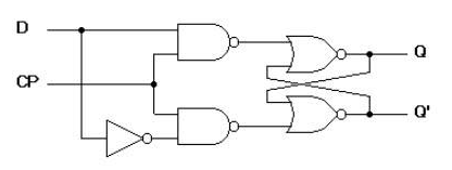
(a) Logic diagram with NAND gates

(b) Graphical Symbol
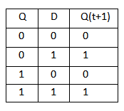
(c) Truth Table
Fig.4 Clocked D Flip-flop
D flip flop is actually a slight modification of the above explained clocked SR flip-flop.
From the figure you can see that the D input is connected to the S input and the complement of the D input is connected to the R input.
The D input is passed on to the flip flop when the value of CP is ‘1’.
When CP is HIGH, the flip flop moves to the SET state. If it is ‘0’, the flip flop switches to the CLEAR state.
J-K Flip Flop
The circuit diagram and truth-table of a J-K flip flop is shown below.
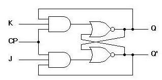
(a) Logic Diagram
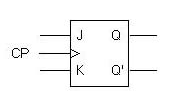
(b) Graphical Symbol

(C) Truth Table
Fig.5 Clocked JK Flip-flop
A J-K flip flop can also be defined as a modification of the S-R flip flop.
The only difference is that the intermediate state is more refined and precise than that of a S-R flip flop.
The behavior of inputs J and K is same as the S and R inputs of the S-R flip flop. The letter J stands for SET and the letter K stands for CLEAR.
When both the inputs J and K have a HIGH state, the flip-flop switch to the complement state. So, for a value of Q = 1, it switches to Q=0 and for a value of Q = 0, it switches to Q=1.
The circuit includes two 3-input AND gates.
The output Q of the flip flop is returned back as a feedback to the input of the AND along with other inputs like K and clock pulse [CP].
So, if the value of CP is ‘1’, the flip flop gets a CLEAR signal and with the condition that the value of Q was earlier 1.
Similarly output Q’ of the flip flop is given as a feedback to the input of the AND along with other inputs like J and clock pulse [CP].
So the output becomes SET when the value of CP is 1 only if the value of Q’ was earlier 1.
The output may be repeated in transitions once they have been complimented for J=K=1 because of the feedback connection in the JK flip-flop.
This can be avoided by setting a time duration lesser than the propagation delay through the flip-flop. The restriction on the pulse width can be eliminated with a master-slave or edge-triggered construction.
Master-Slave Flip Flop
Master-slave flip flop is designed using two separate flip flops. Out of these, one acts as the master and the other as a slave. The figure of a master-slave J-K flip flop is shown below.

Fig.6 Master Slave Flip-flop
From the above figure we can see that both the J-K flip flops are presented in a series connection.
The output of the master J-K flip flop is fed to the input of the slave J-K flip flop.
The output of the slave J-K flip flop is given as a feedback to the input of the master J-K flip flop.
The clock pulse [Clk] is given to the master J-K flip flop and it is sent through a NOT Gate and thus inverted before passing it to the slave J-K flip flop.
Operation
When Clk=1, the master J-K flip flop gets disabled.
The Clk input of the master input will be the opposite of the slave input.
So the master flip flop output will be recognized by the slave flip flop only when the Clk value becomes 0.
Thus, when the clock pulse makes a transition from 1 to 0, the locked outputs of the master flip flop are fed through to the inputs of the slave flip-flop making this flip flop edge or pulse-triggered.
To understand better take a look at the timing diagram illustrated below.

Fig.7 Timing Diagram of Master Slave Flipflop
Thus, the circuit accepts the value in the input when the clock is HIGH, and passes the data to the output on the falling-edge of the clock signal.
This makes the Master-Slave J-K flip flop a Synchronous device as it only passes data with the timing of the clock signal.
T Flip Flop
This is a much simpler version of the J-K flip flop.
Both the J and K inputs are connected together and thus are also called a single input J-K flip flop.
When clock pulse is given to the flip flop, the output begins to toggle.
Here also the restriction on the pulse width can be eliminated with a master-slave or edge-triggered construction. Take a look at the circuit and truth table below.

(a) Logic Diagram
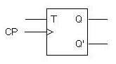
(b) Graphical Symbol
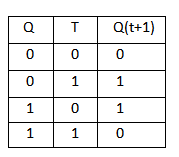
(c) Truth Table