How to Avoid Solder Bridge in PCB Design
Last Updated on May 23, 2019 by Sasmita
Solder Bridge
Have you ever heard of a bridge that doesn’t go anywhere. That means, may be due to some reasons the road project was abandoned and it remained incomplete.
In case of circuit designers, they always wish their bridges to go nowhere. However solder always seems to go where it shouldn’t, and not go where it should.
Solder bridging is just one of the many soldering issues that can occur on your PCB during its manufacturing process.
What is Solder Bridge ?
A solder bridge forms when two or more pads which are not supposed to be electrically connected on a circuit boards , become connected through an excessive application of solder, thus creating a bridge.
This creates an electrical short that can wreak all kinds of havoc, depending on what the two points that are shorted together are designed to do.
Identifying a solder bridge is not easy as this can be microscopic in size. But even the smallest undetected solder bridge on your PCB can lead to some nasty results, like a short circuit or a trace/component burning up.

Fig.1 : Solder bridge being formed between two of the pins of an IC
Why Solder Bridge Occurs ?
So now the question is how this solder is being excessively applied to your board? This is actually the job of a solder mask layer.
This solder resist coating gets added to your PCB during the manufacturing process and is used to protect specific areas of your PCB that should not have solder applied.
For example, the space between two pads on an integrated circuit will be designated with a solder mask, so the only solder you’ll get is on the two pads, but not between them, which could cause a solder bridge.
Some of the most common causes for solder bridging includes:
- Using too much solder on SMT pads because of an incorrect stencil specification.
- Having a bad seal between a stencil and bare board during the printing process.
- Designing solder pads that are too big in relation to the gap between pads.
- Placing components imprecisely or having a reduced component lead to pad size relationship.
- Having an insufficient layer of solder resistance applied between the pads on your board.
How to Avoid Solder Bridge
There are a number of preventative measures that you can take during your design process to stop this solder bridging issue.
Double Check Your Design Rules for Mask Reliefs
A solder mask relief can be defined as an area on your board layout that does not need a solder mask application.
This is most commonly designated as a thin outline surrounding surface mount pads, through-hole pads, test points, and vias.
The solder mask relief is highlighted in green in the image given below :

Fig 2: Solder mask relief surrounding three pads, keeping solder from each component separated.
While setting up your design rules at the start of your project, its always recommend to do a setting of relief between .003” to .008” for all of your SMT components.
However, if your pads are too close together, you might need to adjust this relief value.
If you apply a solder mask relief that leaves no solder mask between each pad, then it’s more likely that it will cause a solder bridge.
The color of the solder mask also influence how extensive your mask reliefs need to be. The chart is given below :

And, you know what, PCBWay doesn’t charge extra fees for different soldermask colors, so feel free to order now.
Always Leave a Solder Mask Dam Between Pads
Another way to prevent Solder bridge is to ensure that you have a solder mask dam between each of your SMT pads.
A solder mask dam acts as isolation wall between the application of solder on each of your pads.
If you don’t have a dam keeping solder contained on a pad, then it can easily spill over onto another pad, causing an unintended solder bridge.
 Fig. 3: Side view of two pads and a solder mask dam separating them on a PCB
It is always recommend setting up solder mask dams between each of the pads on your SMT components.
As a bare minimum, this dam size should always be maintained at .004” (2 mils), otherwise, it becomes very challenging for the manufacturer to isolate solder between pads.
Use Solder Mask Defined Pads For Tight Pitched Areas
In case of very tightly spaced pads on a Ball Grid Array (BGA) or Land Grid Array (LGA), there is not enough room to maintain a barrier and mask relief to have a solder mask dam between two SMT pads.
If such cases, you can use a solder mask defined pad which provides a solder mask relief that’s the same size as the copper pad it is protecting.
To do this you need to make a note in your fabrication files telling your manufacturer to leave the solder mask defined pad as is without applying your standard mask clearances.
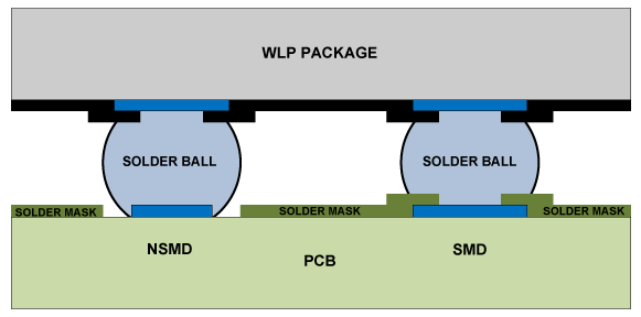
Fig. 4 : A Non-Solder Mask Defined Pad (Left), and A Solder Mask Defined Pad (Right)
Burn The Bridges
Solder mask plays an important role of keeping the components protected and isolated from one another during the application of solder.
And with some healthy boundaries between two pads in the form of solder dams and mask reliefs, you can burn those solder bridges before they ever get a chance to be built.
Final Note : Work with a high-quality PCB assembly house like PCBWay
Though manufacturing process is not in your control, still you can control who you work with.
Since most of the causes of solder bridging are in the build or manufacturing process, work with a trusted and high-quality manufacturer who is willing to show you their process and talk to you about the details. Click here to get an instant quote from PCBWay.com.
![]()
You can do inquiring about how they develop solder paste stencils and how they conduct their board inspection processes.
If you follow the steps above, your solder bridge risk will greatly diminish.
I hope now you are ready to make your design which is sure to be a bridge to future success !