How to reduce PCB Cost
Last Updated on July 7, 2018 by Sasmita
Manufacturing costs of a PCB depend on several factors which must be taken into consideration during the design process.
When you are new in the PCB field, maybe your design is not optimized from a cost point of view.
Normally the majority of beginner PCB designers do not consider basic width, spacing and many other rules that have a big impact not only in the tooling costs but also in the unit prices.
Factors affecting the cost of PCB
In this article we will discuss several recommendations which will help to keep the tooling and manufacturing costs to a minimum.
1. Right Board Size
This is the most obvious rule. Since the cost of a PCB is approximately proportional to the board’s area, the cost tends to go up when the board size is bigger.
Hence, one should try to keep the board size or area to a minimum.
2. Right Board shape
Some PCB fabrication companies charge additional costs for irregular shapes i.e., different from standard shapes such as squares or rectangles.
Figure.1 shows a PCB with an irregular shape.
Fig.1: PCB with an irregular shape
Hence, if the shape of the PCB is not important for the particular design then designing boards with square or rectangular shapes are recommended to reduce the costs.
3. Avoid slots
The PCB fabrication companies also charge extra cost for making slots or internal cutouts on the board.
Hence, if it is not necessary to have slots or internal cutouts for mounting purpose, it is recommended to avoid them. Which in turn will reduce the cost.
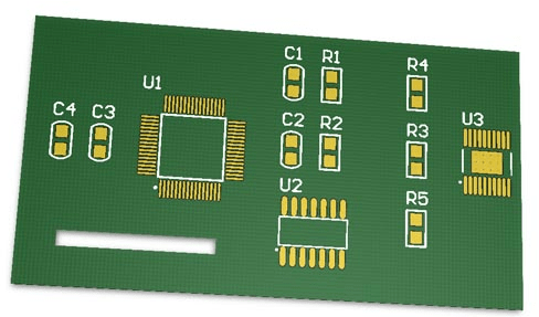
Figure.2 shows a printed circuit board with a rectangular slot.
Fig 2. PCB with a rectangular slot
4. Right Size of copper objects and the spacing between them
The physical dimensions of copper objects and spacing between them is inversely proportional to the cost of PCB.
That means, as the physical dimensions of copper objects and spacing between them decrease, the cost of the PCB increases.
For printing smaller objects on copper, machines with better precision and smaller tolerances are required. Hence, more precision means more cost, and this increase in cost is important especially for low quantities and prototypes.
Here physical dimensions of copper objects refer to pads (SMD and thru-hole), tracks, vias and any object that are printed on a copper layer.
The case of tracks and pads are shown in figure.3 below.
Fig.3 : Spacing between pads and tracks
The spacing between pads is denoted as dP , the spacing between tracks is denoted as dT and the track’s width is denoted as wT.
A standard PCB board is considered to have min(dP), min(dT) and min(wT) in the range of 8 to 10[mils] (0.2[mm] to 0.254[mm] approx). So for reducing costs it would be a good idea to constrain the design to these values.
EDA software generally have a section where you can enter physical rules, which once entered are constantly checked by the DRC (design rule check) system for avoiding out-of-rule errors.
5. Right Sized Holes
In a PCB, the smaller the holes and annular rings, the higher is the price.
Manufacturing smaller holes involves the use of more precise machinery which increases its costs.So we should try to use always the bigger diameter possible for holes.
Some manufacturers charge an extra cost if you need holes smaller than 0.4[mm]. Hence you must ask your PCB manufacturer before determining which is the minimum hole size for an standard PCB ,which does not include any extra cost.Here the hole’s diameter is denoted by dH.
You can check out the PCB Prototype service of PCBWay.com as they do not charge extra fees for PCBs with smaller hole sizes.
There is an important specification known as minimum annular ring which applies only to thru-hole pads and vias.
This is defined as the minimum distance between the hole’s border and the pad’s border.In other words, the minimum width of the copper ring that confines the hole.
This concept is shown in figure.4 and figure.5 below.
Fig.4 : Annular ring concept for a round thru-hole pad or via
Figure .4 shows the minimum annular ring concept for a round thru-hole pad or via .Here it can be noted that the annular ring width is homogeneous around the hole.
The Minimum annular ring concept for an oblong shaped thru-hole pad is shown in figure.5 below.
Fig 5. Minimum annular ring concept for an oblong shaped thru-hole pad
Here in this case the width is not homogeneous around the hole. The minimum annular ring is shown by the red lines in figure.5 .
The PCB cost will be increased if the minimum annular ring is smaller than the standard specifications of the PCB manufacturer.so it is very important to add this rule to the EDA software before designing the PCB.
For example, some manufacturers charge an extra cost if the minimum annular rings smaller than 0.3[mm] are needed. Hence,it is always a good idea to contact the manufacturer and ask them which is the minimum standard value for this variable with no extra cost involved.
6. Choosing the Best Vias
As discussed in the previous article (Basic concepts of PCB) , there are basically 3 types of vias such as through-hole vias, blind vias and buried vias in a PCB.
Blind and buried vias are used for high density and high frequency complex boards and are more expensive than the through-hole vias.
Hence, if it is not necessary,it is recommended to avoid them. Which in turn will reduce the cost.
For buying PCBs at low cost, check out PCBWay’s PCB prototype service (Only $5 for 10 PCBs and every


