Introduction to IC technology
Last Updated on March 26, 2024 by Sasmita
Introduction to IC Technology
The growth of electronics started with invention of vaccum tubes and associated electronic circuits. This activity termed as vaccum tube electronics, subsequently the evolution of solid state devices and consequent development of integrated circuits are responsible for the present status of communication, computing and instrumentation.
Due to its small dimension, low cost, and very high reliability even the common man is familiar with its applications like smart phones and laptops.
The IC’s also found its way in military applications, state of the art communication systems, and industrial applications due to its high reliability and compact size.
Nowadays, an IC that has the size of a fingernail consists of more than a million transistors and other discrete components embedded into it.
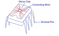
Thus an integrated circuit can also be called a microchip and is basically a collection of some discrete circuits on a small chip that is made of a semiconductor material like silicon.
Integrated circuit
It is a circuit where all discrete components such as passive as well as active elements are fabricated on a single crystal chip
- The first semiconductor chip held two transistors each.
- The first integrated circuits hels only a few devices, perhaps as many as ten diodes, transistors, resistors, and capacitors, making it possible to fabricate one or more logic gates on a single device.
As on increasing the number of components(or transistors) per integrated circuit the technology was developed as:
Small scale integration(SSI)
The technology was developed by integrating the number of transistors of 1-100 on a single chip.
Ex: Gates,flip-flops,op-amps.
Medium scale integration(MSI)
The technology was developed by integrating the number of transistors of 100-1000 on a single chip.
Ex:Counters,MUX, adders, 4-bit microprocessors.
Large scale integration(LSI)
The technology was developed by integrating the number of transistors of 1000-10000 on a single chip.
Ex:8-bit microprocessors,ROM,RAM.
Very large scale integration(VLSI)
The technology was developed by integrating the number of transistors of 10000-1Million on a single chip.
Ex:16-32 bit microprocessors,peripherals,complimentary high MOS.
Ultra large scale integration(ULSI)
The technology was developed by integrating the number of transistors of 1Million-10 Millions on a single chip.
Ex: special purpose processors.
Giant scale integration(GSI)
The technology was developed by integrating the number of transistors of above 10 Millions on a single chip.
Ex:Embedded system, system on chip.
Advantages of Integrated Circuits
Integrated circuits possess the following advantages over discrete circuits:
- Increased reliability due to lesser number of connections.
- Extremely small size due to the fabrication of various circuit elements in a single chip of semiconductor material.
- Lesser weight and space requirement due to miniaturized circuit.
- Low power requirements.
- Greater ability to operate at extreme values of temperature.
- Low cost because of simultaneous production of hundreds of alike circuits on a small semiconductor wafer.
- The circuit layout is greatly simplified because integrated circuits are constrained to use minimum number of external connections.
Disadvantages of Integrated Circuits
- If any component in an IC goes out of order, the whole IC has to b replaced by the new one.
- In an IC, it is neither convenient nor economical to fabricate capacitance exceeding 30 pF. Therefore, for high value of capacitance, discrete components exterior to IC chip are connected.
- It is not possible to fabricate inductors and transformers on the surface of semiconductor chip. Therefore, these components are connected exterior to the semiconductor chip.
- It is not possible to produce high power ICs greater than 10 W.
- There is a lack of flexibilityin an IC i.e. it is generally not possible to modify the parameters within which an integrated circuit will operate.
Types of ICs


Metal-can IC Ceramic flat pack IC 14-Pin Dual In-line Package(DIP) 8-Pin Dual In-line Package(DIP)Plastic
On the basis of applications ICs are of two types namely: Linear Integrated Circuits and Digital Integrated Circuits.
Linear IC’s are used in cases when the relationship between the input and output of a circuit is linear. An important application of linear IC is the operational amplifier commonly referred to as op-amp.
When the circuit is either in on-state or off-state and not in between the two, the circuit is called a digital circuit. IC’s used in such circuits are called digital IC’s. They find wide applications in computers and logic circuits.
Here are some further classification of integrated circuits based on the fabrication techniques used.
- Mono-lithic
- Thin-film
- Thick-film
- Hybrid
1. Monolithic IC
The word ‘monolithic’ comes from the Greek words ‘monos’ and ‘lithos’ which means ‘single’ and ’stone’. As the name suggests, monolithic IC’s refer to a single stone or a single crystal.
The single crystal refers to a single chip of silicon as the semiconductor material, on top of which all the active and passive components needed are interconnected.
This is the best mode of manufacturing IC’ as they can be made identical, and produces high reliability.
The cost factor is also low and can be manufactured in bulk in very less time.
They have been found applicable for C’s used for AM receivers, TV circuits, computer circuits, voltage regulators, amplifiers and so on.

Fig.1 Monolithic IC
Monolithic IC’s have some limitations as well.
1. Monolithic IC’s have low power rating. They cannot be used for low power applications as they cannot have a power rating of more than 1 watt.
2. The isolation between the components inside the IC is poor.
3. Components like inductor cannot be fabricated to the IC.
4. The passive components that are fabricated inside the IC will be if small value. For higher values they have to be connected externally to the IC pins.
5. It is difficult to make a circuit flexible for any kind of variation; a new set of masks is required.
2. Thin and Thick Film Integrated Circuit
Thick and thin film IC’s are comparatively larger than monolithic IC’s and smaller than discrete circuits.
They find their use in high power applications.
Though it is a little large in size, these IC’s cannot be integrated with transistors and diodes.
Such devices have to be externally connected on to its corresponding pins. Passive components like resisters and capacitors can be integrated.
Both thick and thin film IC’s are explained in detailed below.
Though both the IC’s have similar appearance, properties, and general characteristics, the main difference between the two of them is the manner in which the film is deposited on to the IC.
Thin Film Integrated Circuits
This IC is fabricated by depositing films of conducting material on the surface of a glass or ceramic base.
The resistors are fabricated by controlling the width and thickness of the films and by using different materials selected for their resistivity.
For capacitors, a film of insulating oxide is sandwiched between two conducting films.
A spiral form of film is deposited onto the IC to create an inductor.
Mainly two methods are used for producing thin films.
One method, called vacuum evaporation is used in which vaporized material is deposited on a substrate contained in a vacuum.
The other method is called cathode sputtering in which atoms from a cathode made of the desired film material are deposited on a substrate located between a cathode and an anode.
Thick Film Integrated Circuits
They are also commonly called as printed thin film circuits.
The desired circuit pattern is obtained on a ceramic substance by using a manufacturing process called silk-screen printing technique.
The inks used for printing are usually materials that have resistive, conductive, or dielectric properties.They are selected accordingly by the manufacturer.
The screens are actually made of fine stainless steel wire mesh. The films are fused to the substrate after printing by placing them in hot high temperature furnaces.
The fabrication techniques used for thin film passive components are adopted for thick films as well.
As with thin-film circuits, active components are added as separate devices. A portion of thick-film circuit is given in the figure below.

Fig.2 Thick film IC
When compared to monolithic IC’s, thick and thin film IC’s do have some advantages.
They have the advantage of better tolerance, better isolation between components, and greater flexibility in circuit design that further helps in providing high frequency performance.
But, these are the only factors that must be considered for the application of such IC’s as they are costly in making, and has higher dimensions than monolithic IC’s.
They also cannot be used to fabricate active components which further increase the size.
3. Hybrid or Multi-chip Integrated Circuits
As the name suggests, the circuit is fabricated by interconnecting a number of individual chips.
Hybrids ICs are mostly used for high power audio amplifier applications from 5 Watts to more than 50 Watts.
The active components are diffused transistors or diodes.
The passive components may be group of diffused resistors or capacitors on a single chip, or they may be thin-film components.
Interconnection between the individual chips is made by wiring process or a metallized pattern.

Fig.3 Hybrid IC
Hybrid IC’s provide better performance than monolithic IC’s.
Although the process is too expensive for mass production, multi-chip techniques are quite economical for small quantity production and are more often used as prototypes for monolithic ICs.