Maximum Efficiency for Class B Power Amplifier
Last Updated on March 3, 2017 by Sasmita
Maximum Efficiency for Class B Power Amplifier
We have already seen in our previous article about class B power amplifier that a push-pull circuit uses two transistors working in class B operation .
For class B operation, the Q – point is located at cut-off on both d.c. and a.c. load lines .
For maximum signal operation, the two transistors in class B amplifier are alternately driven from cut-off to saturation . This is shown in fig.1 .
Fig.1
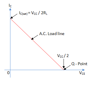
It is clear that a.c. output voltage has a peak value of VCE and a.c. output current has a peak value of IC(sat) .
The same information is conveyed through the a.c. load line for the circuit as shown in fig.2 .
Fig. 2
 Since the two transistors are identical, half the supply voltage is dropped across each transistor’s collector-emitter terminals.
Maximum average a.c. output power Po(max) is
Po(max) = Product of r.m.s. values of a.c. output voltage and a.c. output current
The input d.c. power from the supply VCC is
Where Idc is the average current drawn from the supply VCC .
Since, the transistor is on for alternating half-cycles, it effectively acts as a half-wave rectifier .
Thus, the maximum collector efficiency of class B power amplifier is 78.5% .


