MOSFET Amplifier
Last Updated on January 9, 2020 by Sasmita
An amplifier is an electronics device which raises the strength of a weak signal. In our previous article we discussed how a transistor can function as an amplifier .
In this article we will study how a MOSFET can function as an amplifier.
If we compare between BJT and MOSFET, MOSFET (or, Metal-Oxide-Silicon FET) is an excellent choice for small signal linear amplifiers because of its extremely high input impedance which makes them easy to bias.
But for a MOSFET to produce linear amplification, it has to operate in its saturation region, unlike the Bipolar Junction Transistor (BJT).
But just like the BJT, it too needs to be biased around a centrally fixed Q-point.
Common Source D-MOSFET Amplifier
Fig.1 shows a common-source amplifier using n-channel D-MOSFET. Since the source terminal is common to the input and output terminals, the circuit is called common source amplifier.
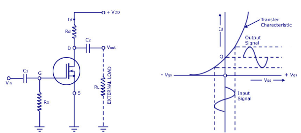
Fig.1
The circuit is zero biased with an a.c. source coupled to the gate through th e coupling capacitor C1 .
The gate is at approximately 0V d.c. and the source terminal is grounded, thus making VGS = 0V .
Operation
The input signal (Vin ) is capacitively coupled to the gate terminal .
In the absence of the signal, d.c. value of VGS = 0V .
When signal (Vin) is applied, Vgs swings above and below its zero value , producing a swing in drain current Id .
- A small change in gate voltage produces a large change in drain current as in JFET . This fact makes MOSFET capable of raising the strength of a weak signal; thus acting as an amplifier.
- During the positive half-cycle of the signal, the positive voltage on the gate increases and produces the enhancement-mode .This increases the channel conductivity and hence the drain current .
- During the negative half-cycle of the signal, the positive voltage decreases and produces depletion-mode. This decreases the conductivity and hence the drain current .
The result of above action is that a small change in gate voltage produces a large change in the drain current.
This large variation in drain current produces a large a.c. output voltage across drain resistance RD .
In this way, D-MOSFET acts as an amplifier .
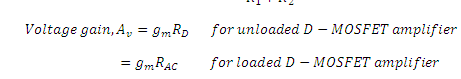
Voltage Gain
The a.c. analysis of D-MOSFET is similar to that of the JFET . Therefore, voltage gain expression derived for JFET are also applicable to D-MOSFET .
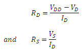
Note that total a.c. drain resistance ;
![]()
Common Source E-MOSFET Amplifier
The construction and operation of Enhancement MOSFET are well explained in this article.
As we know, the Enhancement MOSFETS, or E-MOSFETS, only conduct when a suitable gate-to-source positive voltage is applied, unlike Depletion type MOSFETs which conduct only when the gate voltage is zero.
However, due to the construction and physics of an enhancement type MOSFET, there is a minimum gate-to-source voltage, called the threshold voltage VTh that must be applied to the gate before it starts to conduct, thus allowing the drain current to flow.
In other words, an E-MOSFET does not conduct until the gate-source voltage, VGS is less than the threshold voltage, VTh. .
But as the forward bias at the gate increases, the drain current,ID (or drain-source current,IDS) will also increase, making the E-MOSFET ideal for use in MOSFET amplifier circuits.
Let’s consider the basic E-MOSFET amplifier circuit below.
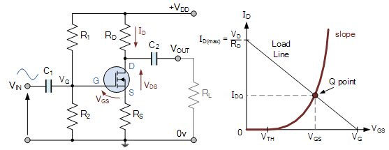
This simple enhancement-mode common source MOSFET amplifier configuration uses a single supply at the drain and generates the required gate voltage, VG using a resistor divider.
As we know that for a MOSFET, no current flows into the gate terminal, we can make the following basic assumptions about the MOSFET amplifiers DC operating conditions .
 Hence we can say that :
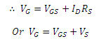
and the MOSFET gate-to-source voltage, VGS is given as:
![]()
As we have already discussed, for proper operation of the mosfet, this gate-source voltage must be greater than the threshold voltage of the MOSFET, that is VGS > VTH.
Since IS = ID, the gate voltage, VG is therefore equal too:
![]()
To set the MOSFET amplifier gate voltage to this value we select the values of the resistors, R1 and R2 within the voltage divider network to the required values.
Since, no current flows into the gate terminal of a MOSFET device so the formula for voltage division is given as:
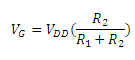
It can be noted that, this voltage divider equation only determines the ratio of the two bias resistors, R1 and R2 and not their actual values.
It is always desirable to make the values of these two resistors as large as possible to reduce their I2R power loss and increase the MOSFETs amplifiers input resistance.