How to create a PCB Design
Last Updated on July 7, 2018 by Sasmita
PCBs are some of the most common things you will see, if you are into electronics . These boards make our lives easier by eliminating all those connecting wires and breadboards.
If properly designed, it will reduce the size of your device to a large extend.
What is a PCB ?
Basically a printed circuit board (PCB) mechanically supports and electrically connects electronic components using conductive tracks, pads, and other features etched from copper sheets laminated onto a non-conductive substrate.
It has pre-designed copper tracks on a conducting sheet. The pre-defined tracks reduce the wiring and thereby reduces the faults arising due to loose connections.One simply needs to place the components on the PCB and solder them.
In this tutorial, we will discuss the process of designing a PCB layout and getting it printed by a custom PCB manufacturer.
When you are going to design your own PCB, you need to draw holes, pads and wires for your circuit. Then you send this drawing to a manufacturer or you can etch it yourself.But that method is very messy and it uses a lot of chemicals. So it is much easier (and cheaper) to get your PCB made by a professional manufacturer.
Start with schematics
Before you start drawing wires and stuff, first you need to know what circuit you want to build.
So you need to design schematics for your circuit.For this you need a PCB design software.
Then you are ready to begin the process.
Start by drawing your schematic diagram into the software you have chosen. (You can use free PCB design tool such as EasyEDA )
Start by logging in to EasyEDA, and create a new project:

Once you’re on the Start page, click on the “new Schematic” tab:

Now you’ll see a blank canvas where you can draw the schematic:

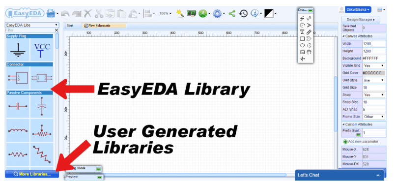
In EasyEDA, schematic symbols are located in “Libraries”. The default EasyEDA library has most of the common symbols, but there are also “User Generated Libraries” with lots of other symbols:
Each schematic symbol you use needs to have a PCB footprint associated with it. The PCB footprint will define the component’s physical dimensions and placement of the copper pads or through holes. Now is a good time to decide which components you’ll be using.
The schematic symbols in the EasyEDA library already have footprints associated with them, but they can be changed if your’re using a different size or style:

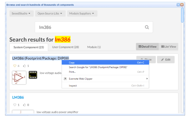
To change the footprint associated with a schematic symbol, search in the “User Generated” libraries for a footprint that matches the component you’re using. Once you find it, click on the heart icon to “Favorite” it:

Then copy the name of the component:
Now click on the symbol in the schematic editor, and paste the name of the new footprint into the “package” field in the right sidebar menu.

Once all of your symbols are placed on the schematic and you’ve assigned footprints to each symbol, it’s time to start drawing the wires.
After all the wiring is done, it’s a good idea to label the symbols. The labels will be transferred over to the PCB layout and eventually be printed on the finished PCB. Each symbol has a name (R1, R2, C1, C2 etc.) and value (10 μF, 100 Ω, etc.) that can be edited by clicking on the label.
The next step is to import the schematic into the PCB editor.
Create PCB Layout
Now let’s see how to layout a PCB in EasyEDA.
Open your schematic in the schematic editor, and click on the “Convert Project To PCB” button:

The footprints associated with each schematic symbol will be automatically transferred to the PCB editor:

The thin blue lines connecting the components are called ratsnest lines. Ratsnest lines are virtual wires that represent the connections between components. They show you where you need to route the traces according to the wiring connections you created in your schematic:

Now you can start arranging the components. You might want to do some research to find out if there are any special design requirements for your circuit. Some circuits perform better with certain components in specific locations. For example, in an LM386 amplifier circuit the power supply decoupling capacitors need to be placed close to the chip to reduce noise.
After you’ve arranged all of the components, it’s time to start drawing the traces. Use the ratsnest wires as a rough guide for routing each trace. However, they won’t always show you the best way to route the traces, so it’s a good idea to refer back to your schematic to verify the correct connections.
Traces can also be routed automatically using the software’s auto-router. For complicated circuits, it’s generally better to route traces manually, but try the auto-router on simpler designs and see what it comes up with. You can always adjust individual traces later.

Now it’s time to define the size and shape of the PCB outline. Click on the board outline and drag each side until all of the components are inside:

The last thing to do before placing the order is to run a design rule check. A design rule check will tell you if any components overlap or if traces are routed too close together. The design rule check can be found by clicking the “Design Manager” button in the right side window:

Items that fail the design rule check will be listed below the “DRC Errors” folder. If you click on one of the errors, the problem trace or component will be highlighted in the PCB view:

You can specify your own settings for the design rule check by clicking the drop down menu in the upper right hand corner and going to Miscellaneous > Design Rule Settings:

This will bring up a window where you can set design rules for trace width, distance between traces, and other useful parameters:

At this point it’s a good idea to double check your PCB layout against your schematic to make sure that everything is connected properly. If you’re satisfied with the result, the next step is to order the PCB.
Order the PCB
Start by clicking the “Fabrication Output” button in the top menu of the PCB editor:

This will take you to another PCB order page where you can download or view gerber files of your PCB and send them to any manufacturer.

Gerber files are a set of image files that contain the patterns used to manufacture your PCB. All of the files are compressed into a single .zip file. There is a separate file for the copper traces, silk screen, and locations of drill holes and vias:

You can check out PCBWay.com for Project Sponsorship, as they have some good offers out there. In fact, you can even make some commissions if you share your open source projects.
And if you love designing PCBs, you can participate in PCB Design Contests organized by PCBWay.com. They offer some great cash prizes over there.