PCB Fiducial Mark
Last Updated on August 9, 2018 by Jhasketan Garud
PCB Fiducial Mark
Fiducial Marks are a feature of the printed circuit board (PCB) artwork, which provides common measurable points for all steps in the assembly process. This allows all automated assembly equipment to accurately locate the circuit pattern.
Fig.1: Fiducial Mark
Fiducial marks come into play when a PCB is assembled by an automated pick and place machinery which are basically robots that put the components on the board.
These robots require incredible precision to accurately place the components on the PCB. For example a 0201 size resistor or 2mm x 2mm chip scale micro BGA.
For buying PCBs at low cost, check out PCBWay’s PCB prototype service (Only $5 for 10 PCBs and every
A fiducial mark is an alignment mark for surface mount assembly machines.
The marks ensure that your board is oriented in the correct direction and aligned as close to perfect as possible.
Assembly machines use cameras to locate fiducial marks, and then adjust component placement based on the exact position of the board. The whole process typically requires more than one fiducial mark in a non-reversible pattern.
Fiducial Marks are generally categorized in two types:
- Global Fiducials
- Local Fiducial
Global Fiducials
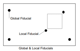
These are the Fiducial marks used to locate the position of all features on an individual printed circuit board. When multiple boards are processed as a panel, the global fiducials may also be referred to as panel fiducials if used to locate the circuits from the panel data.
Global or panel fiducials should ideally be located on a three point grid-based system, with the lower left fiducial located at the 0,0 point and the other two fiducials located in the positive X and Y directions.
Global fiducials should be located on all PCB layers that contain components to be mounted with automated equipment.
Fig.2: Global and Panel Fiducial Mark
Local Fiducials
These are the Fiducial marks used to locate the position of an individual component that may require more precise location, such as a .020” pitch QFP.
All Fine Pitch components should have two local fiducials designed into the land pattern of the component.
Fig.3: Global and Local Fiducial marks
When to Use a Fiducial Mark
High volume assembly always requires fiducial marks to ensure accurate registration and parts placement.
However, low volume assembly does not always require them.
Even if fiducial marks are not required for assembling your particular product, they still help and are always a good idea.
The only time that you can know for sure that fiducial marks are unnecessary is when you are placing your parts by hand.
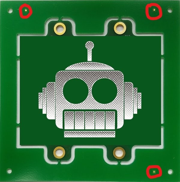
In the image below, you can see three small metal dots (upper left, upper right, and lower right areas of the board). Those are the fiducial marks. If the electronics for this board were being placed by hand, the marks would not be necessary. However, because hundreds of copies of this board are being produced in an assembly line, it is important that the machines know the difference between the top/bottom and sides of the board. You do not want the electronics placed in a way that does not follow the designated pattern.
Fig.4
Fiducial Mark Design Guidelines
Two things that are most important in the construction of fiducial marks are:
- position accuracy
- contrast
Position Accuracy
A fiducial must be created in the top copper layer.
One must think why copper?? When theoretically using a silk screen or drill hole would work!
Well, the answer is registration. All of the top copper is put down in one operation. Therefore, positional accuracy of a surface mount pad relative to a copper fiducial will always be the same.
Silk screen and drill holes are added in separate operations, so there is always a chance that registration will vary from board to board.
A typical 0.4mm pitch BGA has a pad size of .254 mm (.01”), and has a space of .15 mm (.0059”) between pads. Silkscreen and drill holes simply do not have the precision needed for alignment at those geometries.
Contrast
The cameras in the machine need good contrast, which is why the mark has to be bare copper.
Solder mask on top of a copper pad will lower the contrast to the point that the camera may not be able to see it.
Solder mask has the same registration issues as silkscreen, so you need to make sure that no part of the pad is obscured.
Make the copper pad 1 to 2 mm in diameter. The mask opening should be 2 – 5 mm larger than the copper.
Some CAD packages have fiducial marks in their components library. That would be the easiest route.
Shape of a Fiducial Mark
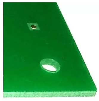
The image below shows closeup detail of a fiducial used on the board shown above.
Fig.5
This particular fiducial mark uses a square cutout in the silk screen. Most use a round cutout, but the shape is not all that important. However, the copper pad should be round.
Size of Fiducial Marks
The size of fiducial mark depends on the assembly machines.
Dimensions of 3.2mm solder mask opening diameter and 1.6mm diameter of bare copper or 2mm solder mask opening diameter and 1mm diameter of bare copper are excellent for almost all Assembly machines.
The image below shows dimensions of the fiducial marks.
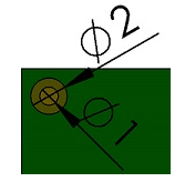 Fig.6:Dimensions of Fiducial marks
How many and where to position Fiducial Marks
If you have SMD components on both sides of the PCB you need to place it on both sides top and bottom of your layout.
There are not any strict rules for the number of fiducial marks. However, it is good to position two fiducial marks on opposite corners of the PCB near corner edges.
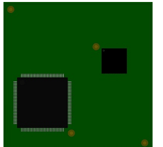
If you have BGA, QFN, QFP packages with small pitch on the layout, it is very useful to position one fiducial mark near every one of those packages/footprints.
The Fig.7 below shows positions of the fiducial marks on the board with one QFN and one QFP package with small pitch.
Fig.7: Positions of the fiducial marks on the PCB
It is also helpful and sometimes necessary to place four fiducial markers near panel corners. However, it also depends on the assembly machine.
Fig.8 shows positions of the fiducial marks on the panel edge.
Fig.8: Positions of the fiducial marks on the panel edge
For buying PCBs at cheap rates check out PCBWay.com.


