Single Stage Transistor Amplifier
Last Updated on January 9, 2020 by Sasmita
Single Stage Transistor Amplifier
When in an amplifier circuit only one transistor is used for amplifying a weak signal, the circuit is known as single stage amplifier.
However, a practical amplifier consists of a number of single stage amplifiers and hence a complex circuit. Therefore, such a complex circuit can be conveniently split into several single stages and can be effectively analysed.
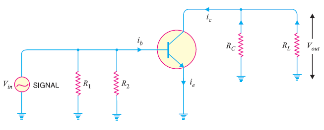
The above fig. shows a single stage transistor amplifier.
When a weak a.c. signal is applied to the base of the transistor, a small base current starts flowing in the input circuit.
Due to transistor action, a much larger (β times the base current) a.c. current flows through the the load Rc in the output circuit.
Since the value of load resistance Rc is very high, a large voltage will drop across it.
Thus, a weak signal applied in the base circuit appears in amplified form in the collector circuit. In this way the transistor acts as an amplifier.
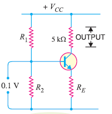
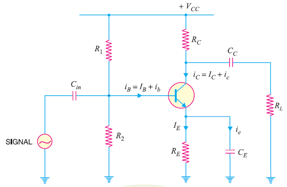
Practical Circuit of Transistor Amplifier
To achieve faithful amplification in a transistor amplifier, we must use proper associated circuitry with the transistor.
A practical single stage transistor amplifier circuit is shown in fig. below.
The various circuit elements and their functions are described as follows :
(i) Biasing Circuit
The resistances R1 , R2 and RE provide biasing and stabilisation.
The biasing circuit must establish a proper operating point otherwise a part of the negative half cycle of the signal may be cut off in the output and you will get faithful amplification.
(ii) Input Capacitor (Cin)
An electrolytic capacitor of value 10 μF is used to couple the signal to the base of the transistor.
Otherwise, the signal source resistance will come across R2 and thus can change the bias.
This capacitor allows only the a.c. signal to flow but isolates the signal source from R2 .
(iii) Emitter Bypass Capacitor (CE)
An emitter bypass capacitor of value 100 μF is used in parallel with RE to provide a low reactance path to the amplified a.c. signal.
If this capacitor is not connected in the output circuit then the amplified a.c. signal will flow through RE and cause a voltage drop across it, thereby reducing the output voltage.
(iv) Coupling Capacitor (CC)
The coupling capacitor of value 10 μF is used to couple one stage of amplification to the next stage.
If it is not used, the bias condition of the next stage will be drastically changed due to the shunting effect of RC . This is because RC will come in parallel with the resistance R1 of the biasing circuit of the next stage amplifier circuit and hence, alter the biasing condition of the next stage.
Therefore, the coupling capacitor is used to isolates the d.c. of one stage from the next stage and allows the a.c. signal only.
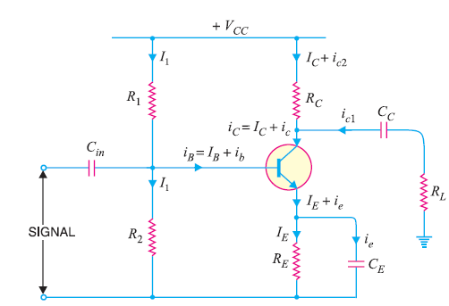
Various Circuit Currents
(i) Base Current
When no signal is applied in the base circuit, d.c. base current IB, also known as zero signal base current flows due to the biasing circuit.
When a.c. signal is applied, a.c. base current ib flows in the base circuit.
Hence, the total base current iB is given by :
![]()
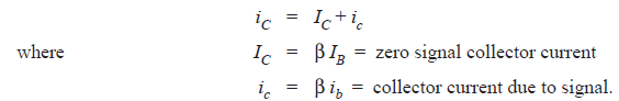
(ii) Collector Current
When no signal is applied, a d.c. collector current IC, also known as zero signal collector current flows due to the biasing circuit.
When a.c. signal is applied, a.c. collector current ic also flows in the collector circuit.
Hence, the total collector current iC is given by :
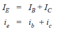
(iii) Emitter Current
When no signal is applied, a d.c. emitter current IE, flows due to the biasing circuit.
When a.c. signal is applied, a.c. emitter current ie also flows .
Hence, the total emitter current iE is given by :
![]()
It is useful to keep in mind that :
Now base current is usually very small, therefore, we can take the approximation :
![]()
D.C. and A.C. Equivalent Circuits
To analyse the action of a transistor in a simple way, the analysis is divided into two parts such as; d.c. analysis and a.c. analysis.
In d.c. analysis, we will consider all the d.c. sources at the same time and work out the d.c. currents voltages in the circuit.
Similarly, in a.c. analysis, we will consider all the a.c. sources at the same time and work out the a.c. currents and voltages .
For this analysis let us consider the amplifier circuit shown in fig. below .
(1) D.C. Equivalent Circuit
In the d.c. equivalent circuit of a transistor amplifier, only d.c. conditions must be considered.
So let us assume there is no signal applied to the circuit.
Since, d.c. currents can not pass through the capacitors, hence, all the capacitors look like open circuits in the d.c. equivalent circuit.
Therefore, to draw the d.c. equivalent circuit, the following two steps are applied to the transistor amplifier circuit :
- Make all the a.c. sources zero/Remove all the a.c sources
- Open all the capacitors
Applying these two steps to the circuit shown in fig.3, we will get the d.c. equivalent circuit as shown in fig. below.
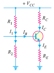
Now we can easily calculate the d.c. currents and voltages from this circuit.
(2) A.C. Equivalent Circuit
In the a.c. equivalent circuit of a transistor amplifier, only a.c. conditions must be considered.
In this case, d.c. voltage is not so important hence, may be assumed to be zero.
The capacitors are used in the circuit to couple or bypass the a.c. signal.
The capacitors are generally taken of large values so as to appear as short circuits to the a.c. signal.
Therefore, to draw the a.c. equivalent circuit, the following two steps are applied to the transistor amplifier circuit :
- Make all the d.c. sources zero/Remove all the d.c. sources
- Short all the capacitors
Applying these two steps to the circuit shown in fig.3, we will get the a.c. equivalent circuit as shown in fig. below.
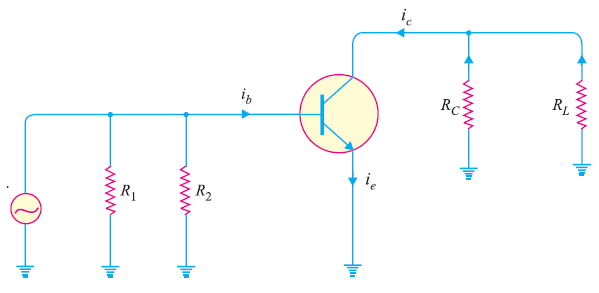
Now we can easily calculate the a.c. currents and voltages from this circuit.
Voltage Gain of Single stage Transistor Amplifier
The voltage gain of a single stage transistor amplifier is the ratio of a.c. output voltage to a.c. input signal voltage.
Hence, in order to determine the voltage gain, you should consider only the a.c. currents and voltages in the circuit. In other words you have to consider the a.c. equivalent circuit of the transistor amplifier.
The a.c. equivalent circuit of a transistor amplifier is shown in fig. below.
As far as a.c. signal is concerned, load RC appears in parallel with RL.
Therefore, the effective load resistance for a.c. is given by :
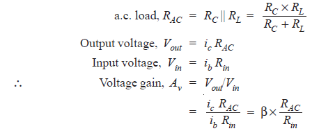
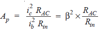
Incidentally, power gain is given by :