How Smart Fabs Revolutionize Semiconductor Manufacturing: Benefits and Innovations
Introduction
The semiconductor industry lies at the heart of modern technology, powering everything from smartphones and laptops to cars and advanced medical equipment. As demand for smaller, faster, and more energy-efficient chips grows, manufacturers face immense pressure to increase productivity while reducing costs and defects. This is where smart fabs—semiconductor fabrication plants equipped with advanced automation, data analytics, and AI—are transforming the landscape.
Smart fabs integrate cutting-edge technologies like Industrial IoT (IIoT), artificial intelligence (AI), machine learning (ML), robotics, and digital twins to optimize every stage of semiconductor production. By leveraging these innovations, manufacturers are achieving higher yields, greater efficiency, and improved reliability.
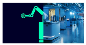
Pic Courtesy : Siemens
What is a Smart Fab?
A smart fab is an intelligent, connected, and highly automated semiconductor manufacturing facility that uses real-time data and advanced analytics to drive decision-making. Unlike traditional fabs, which rely heavily on manual monitoring and reactive maintenance, smart fabs are proactive, adaptive, and self-optimizing.
Key features of a smart fab include:
-
IoT-enabled sensors for real-time equipment and process monitoring.
-
Automated material handling systems for seamless wafer movement.
-
AI and ML algorithms for defect detection and yield prediction.
-
Digital twin technology to simulate, optimize, and test processes virtually.
-
Predictive maintenance to minimize downtime and extend equipment life.
Benefits of Smart Fabs in Semiconductor Manufacturing
1. Higher Yield and Fewer Defects
-
AI-driven analytics detect minute process variations that human operators may overlook.
-
Real-time adjustments during lithography, etching, and deposition reduce wafer defects.
-
Machine learning models predict yield outcomes, enabling manufacturers to optimize recipes before full-scale production.
2. Increased Operational Efficiency
-
Automated guided vehicles (AGVs) and robotic arms transport wafers efficiently.
-
Smart scheduling systems minimize bottlenecks in complex fabrication workflows.
-
Continuous monitoring reduces rework and scrap, saving time and resources.
3. Predictive and Preventive Maintenance
-
IoT sensors track vibration, temperature, and pressure in equipment.
-
Predictive analytics forecast potential failures before they occur.
-
This reduces unplanned downtime and maximizes equipment utilization.
4. Energy and Resource Optimization
-
Smart fabs monitor energy consumption and identify inefficiencies.
-
Automated control of HVAC, cleanrooms, and power systems lowers operating costs.
-
Advanced recycling and reuse of chemicals and water support sustainability goals.
5. Faster Time-to-Market
-
Digital twins simulate new process flows, reducing trial-and-error experiments.
-
AI-powered insights accelerate process optimization and product development.
-
Manufacturers can respond quickly to market demands, such as high-performance chips for AI and 5G.
6. Scalability and Flexibility
-
Modular and software-driven operations allow fabs to adapt to new chip designs.
-
Smart fabs can switch production lines efficiently without major infrastructure changes.
How A Smart Factory Can Improve Traditional Manufacturing Processes
A semiconductor company needs to look into the following to add smart manufacturing process methods into their fabrication plant. Along with the opportunities to optimize production and improve yield, there are plenty of challenges as well.
The Digital Twin Concept
A digital twin of the semiconductor fabrication plant is essentially a virtual system that can be used to run simulations. This concept of a digital twin is heavily used in industries such as aerospace, defense, and automotive to describe the as-designed product. Many of the modern equipment used during production already comes with 3D models and detailed specifications of how it’s supposed to work. Engineers have also come up with models that simulate manufacturing processes. Together, these models can be utilized to simulate the flow of production, and processes within it, and forecast the results.
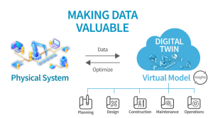
Pic Courtesy : Tributech Solution
Once a digital twin of the fabrication plant is established, specific parameters like the mix of products, materials, and even customer supply orders can be tweaked to run simulations. The optimum settings for new equipment and operating procedures can be discovered to improve yield. The time taken from the prototype stage to full production can be reduced as well.
A digital twin’s simulations can be further improved by feeding it data from the MES as well as maintenance, testing, and scheduling operations. This can allow manufacturers a way to understand their factory’s performance in real time. Naturally, running these digital twin simulations requires advanced computing with statistical modeling and machine learning capabilities as well as simulation software.
A Manufacturing Execution System With Improved Scheduling
The manufacturing execution system or MES of a semiconductor fabrication plant is the software that does the monitoring, documentation, and controls the entire production line from raw materials to the finished product. These systems arose as the need for compliance grew in highly regulated industries like aerospace and medical, requiring methods for traceability in case a faulty product needed to be recalled. This need exists within the semiconductor industry as well.
Conventional MES connected to scheduling systems allow for basic product planning across a scale of months or days, which gives production teams an idea of the production volume required, the deadlines to be met, as well as resources and materials needed to produce it. However, since the product mix manufactured at a plant is always changing, the production team on the current shift needs constant updates on what needs to be done. Finite production scheduling is increasingly being required at the shift or even hourly level.
With a smart manufacturing approach, new MES is being developed with built-in scheduling, unlike the older models that often had limited or zero integration with their scheduling applications. This allows for testing to be conducted without delaying ongoing production, and the production team on the current shift gets detailed views of resource constraints, priorities as well as what needs to be done at the workstation level.
Real-World Applications
-
TSMC, Intel, and Samsung are investing heavily in smart fab technologies to stay ahead in the semiconductor race.
-
AI-powered defect detection tools are already reducing inspection times in advanced nodes below 5 nm.
-
Digital twin models are being used to optimize extreme ultraviolet (EUV) lithography processes.
Challenges Ahead
Despite their advantages, smart fabs face challenges:
-
High investment costs for infrastructure and AI integration.
-
Cybersecurity risks due to increased connectivity.
-
Talent gaps in AI, data science, and semiconductor engineering.
Addressing these hurdles will require strong partnerships between semiconductor companies, technology providers, and governments.
Conclusion
Smart fabs represent the future of semiconductor manufacturing, enabling companies to achieve unprecedented efficiency, yield, and agility. By harnessing IoT, AI, digital twins, and predictive analytics, smart fabs are not just improving chip production—they are revolutionizing it. In an era where every nanometer counts, the shift toward intelligent, connected manufacturing is ensuring that the semiconductor industry keeps pace with the world’s insatiable demand for advanced electronics.