This article presents a series of solved problems on Field Effect Transistors (FETs) to help students understand their working principles, characteristics, and applications in electronic circuits
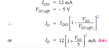
Q1. Fig. 1 shows the transfer characteristic curve of a JFET. Write the equation for drain current.
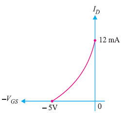
Fig.1
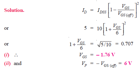
Solution. Referring to the transfer characteristic curve in Fig. 1, we have,
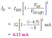
Q2. A JFET has the following parameters: IDSS = 32 mA ; VGS (off) = – 8V ; VGS = – 4.5 V. Find the value of drain current.
Solution :
Q3. A JFET has a drain current of 5 mA. If IDSS = 10 mA and VGS (off) = – 6 V, find the value of (i) VGS and (ii) VP.
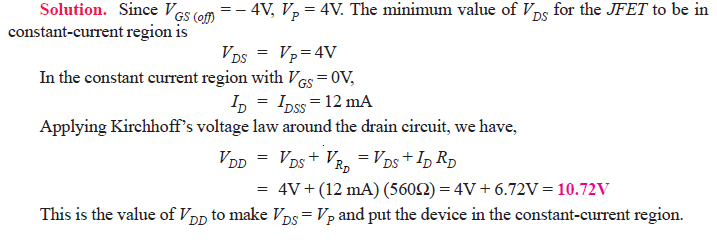
Q4. For the JFET in Fig. 2, VGS (off) = – 4V and IDSS = 12 mA. Determine the minimum value of VDD required to put the device in the constant-current region of operation.
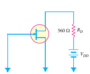
Fig.2
Q5. Determine the value of drain current for the circuit shown in Fig. 3.
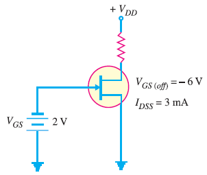
Fig.3
Solution. It is clear from Fig. 3 that VGS = – 2V. The drain current for the circuit is given by;
Q6. When a reverse gate voltage of 15 V is applied to a JFET, the gate current is 10−3 μA. Find the resistance between gate and source.
Solution.
![]()

Q7. When VGS of JFET changes from –3.1 V to –3 V, the drain current changes from 1 mA to 1.3 mA. What is the value of transconductance?

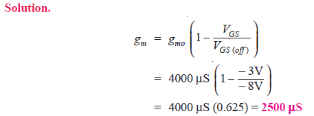
Q8. A JFET has a value of gmo = 4000 μS. Determine the value of gm at VGS = – 3V. Given that VGS (off) = – 8V.
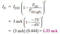
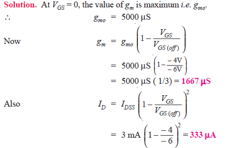
Q9. The datasheet of a JFET gives the following information: IDSS = 3 mA, VGS (off) = – 6V and gm (max) = 5000 μS. Determine the transconductance for VGS = – 4V and find drain current ID at this point.
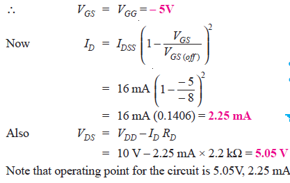
Q10. A JFET in Fig. 4 has values of VGS (off) = – 8V and IDSS = 16 mA. Determine the values of VGS, ID and VDS for the circuit.
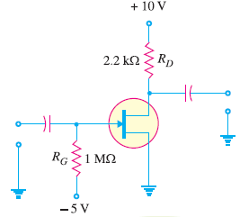
Fig. 4
Solution.
Since there is no gate current, there will be no voltage drop across RG.
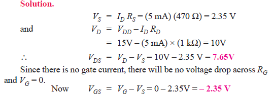
Q11. Find VDS and VGS in Fig. 5, given that ID = 5 mA.
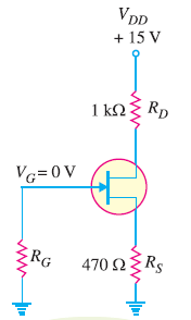
Fig. 5
Q12. The transfer characteristic of a JFET reveals that when VGS = – 5V, ID = 6.25 mA. Determine the value of RS required.
Solution.

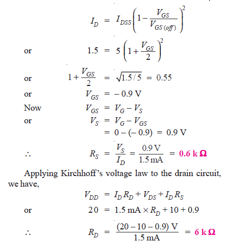
Q13. Determine the value of RS required to self-bias a p-channel JFET with IDSS = 25 mA, VGS (off) = 15 V and VGS = 5V.
Solution.

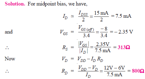
Q14. Select resistor values in Fig. 6 to set up an approximate midpoint bias. The JFET parameters are : IDSS = 15 mA and VGS (off) = – 8V. The voltage VD should be 6V (one-half of VDD).
 Fig.6
Fig.6
Q15. In a self-bias n-channel JFET, the operating point is to be set at ID = 1.5 mA and VDS =10 V. The JFET parameters are IDSS = 5 mA and VGS (off) = − 2 V. Find the values of RS and RD. Given that VDD = 20 V.
Solution. Fig. 7 shows the circuit arrangement.
 Fig.7
Fig.7
Q16. In the JFET circuit shown in Fig. 8, find (i) VDS and (ii) VGS.
Fig.8

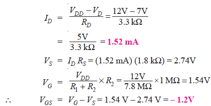
Q17. Determine ID and VGS for the JFET with voltage-divider bias in Fig. 9, given that VD = 7V.
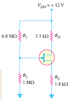
Fig.9
Solution.
Q18. In an n-channel JFET biased by potential divider method, it is desired to set the operating point at ID = 2.5 mA and VDS = 8V. If VDD = 30 V, R1 = 1 MΩ and R2 = 500 kΩ, find the value of RS. The parameters of JFET are IDSS = 10 mA and VGS (off) = – 5 V.
Solution. Fig. 10 shows the conditions of the problem.
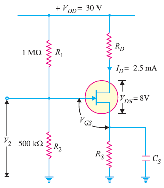
Fig.10
Q19. Draw the d.c. load line for the JFET amplifier shown in Fig. 11.
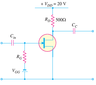
Fig.11
Solution.
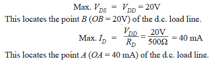
Fig. 12 shows the d.c. load line AB.
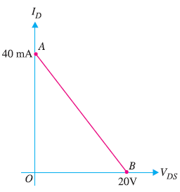
Fig.12
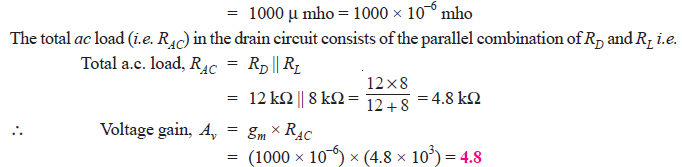
Q20. The JFET in the amplifier of Fig. 13 has a transconductance gm = 1 mA/V. If the source resistance RS is very small as compared to RG, find the voltage gain of the amplifier.
Fig.13
Solution.
Transconductance of JFET, gm= 1 mA/V
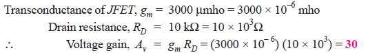
Q21. The transconductance of a JFET used as a voltage amplifier is 3000 μmho and drain resistance is 10 kΩ. Calculate the voltage gain of the amplifier.
Solution.
Q22. What is the r.m.s. output voltage of the unloaded amplifier in Fig. 14? The IDSS = 8 mA, VGS (off) = – 10V and ID = 1.9 mA.
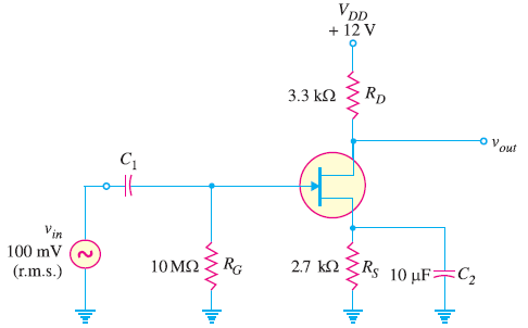
Fig.14
Solution.
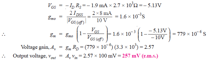
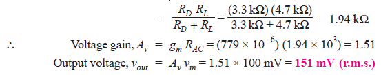
Q23. If a 4.7 kΩ load resistor is a.c. coupled to the output of the amplifier in Fig. 15 , what is the resulting r.m.s. output voltage?
Fig.15
Solution.
The value of gm remains the same. However, the value of total a.c. drain resistance RAC changes due to the connection of load RL (= 4.7 kΩ).
Total a.c. drain resistance, RAC = RD || RL
Q24. In a JFET amplifier, the source resistance RS is unbypassed. Find the voltage gain of the amplifier. Given gm = 4 mS; RD = 1.5 kΩ and RS = 560Ω.
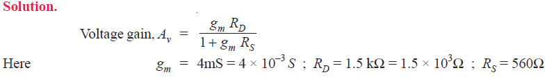
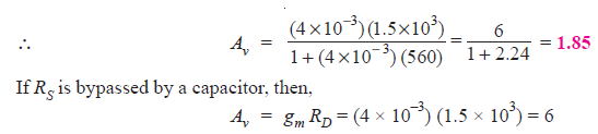
Thus with unbypassed RS, the gain = 1.85 whereas with RS bypassed by a capacitor, the gain is 6. Therefore, voltage gain is reduced when RS is unbypassed.
Q25. For the JFET amplifier circuit shown in Fig. 16, calculate the voltage gain with (i) RS bypassed by a capacitor (ii) RS unbypassed.
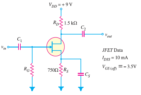
Fig.16

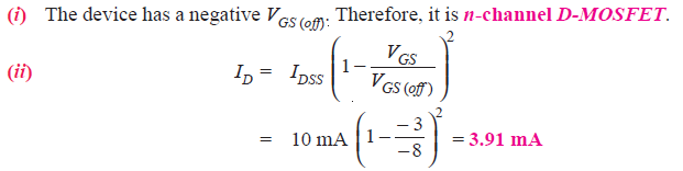
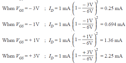
Q26. For a certain D-MOSFET, IDSS = 10 mA and VGS (off) = – 8V.
(i) Is this an n-channel or a p-channel ?
(ii) Calculate ID at VGS = – 3V.
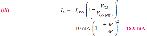
(iii) Calculate ID at VGS = + 3V.
Solution.
Q27. A D-MOSFET has parameters of VGS (off) = – 6V and IDSS = 1 mA. How will you plot the transconductance curve for the device?
Solution.
When VGS = 0 V, ID = IDSS = 1 mA and when VGS = VGS (off), ID = 0A. This locates two points viz IDSS and VGS (off) on the transconductance curve. We can locate more points of the curve by changing VGS values.
Thus we have a number of VGS – ID readings so that transconductance curve for the device can be readily plotted.
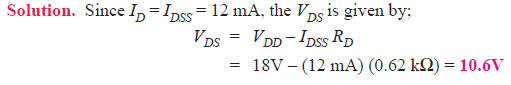
Q28. Determine the drain-to-source voltage (VDS) in the circuit shown in Fig. 17 if VDD = +18V and RD = 620Ω. The MOSFET data sheet gives VGS (off) = – 8V and IDSS = 12 mA.
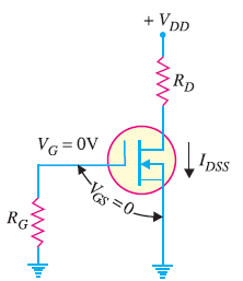
Fig.17
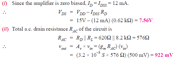
Q29. The D-MOSFET used in the amplifier of Fig. 18 has an IDSS = 12 mA and gm = 3.2 mS. Determine (i) d.c. drain-to-source voltage VDS and (ii) a.c. output voltage. Given vin = 500 mV.
Fig.18
Solution.
Q30. The data sheet for an E-MOSFET gives ID(on) = 500 mA at VGS = 10V and VGS (th) = 1V. Determine the drain current for VGS = 5V.
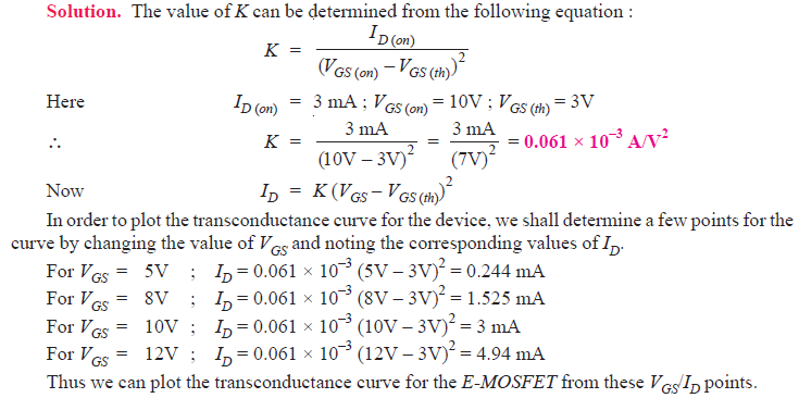
Q31. The data sheet for an E-MOSFET gives ID (on) = 3 mA at VGS = 10V and VGS (th)= 3V. Determine the resulting value of K for the device. How will you plot the transconductance curve for this MOSFET ?
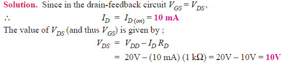
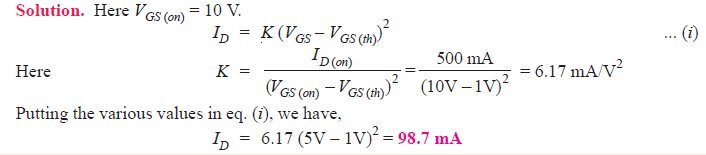
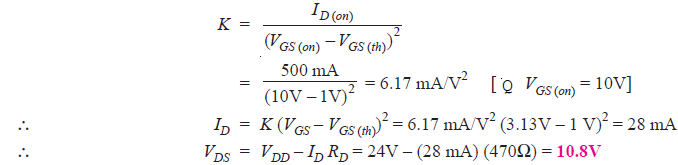
Q31. Determine VGS and VDS for the EMOSFET circuit in Fig. 19. The data sheet for this particular MOSFET gives ID (on) = 500 mA at VGS = 10V and VGS (th) = 1V.
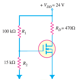
Fig.19
Solution. Referring to the circuit shown in Fig. 19, we have,
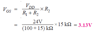
The value of K can be determined from the following equation :
Q32. Determine the values of ID and VDS for the circuit shown in Fig. 20. The data sheet for this particular MOSFET gives ID (on) = 10 mA when VGS = VDS.
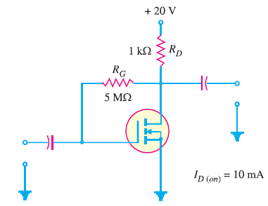
Fig.20