Q1. If the d.c. output voltage is 400V with no-load attached to power supply but decreases to 300V at full-load, find the percentage voltage regulation.
Q2. A power supply has a voltage regulation of 1%. If the no-load voltage is 30V, what is the full-load voltage ?
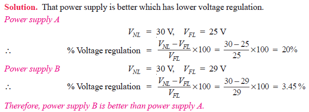
Q3. Two power supplies A and B are available in the market. Power supply A has no-load and full-load voltages of 30V and 25V respectively whereas these values are 30V and 29V for power supply B. Which is a better power supply?
Q4. Fig. 1 shows the regulation curve of a power supply. Find
(i) voltage regulation and
(ii) minimum load resistance.
Fig.1
Solution :
Referring to the regulation curve shown in Fig. 1, it is clear that :
Q5. In adding 1A load to an existing 1A load, the output voltage of a power supply drops from 10.5V to 10V. Calculate (i) output impedance of power supply and (ii) no-load voltage of power supply.
Solution.
All practical power supplies always have some internal impedance (often called output impedance) which is denoted by Zo as shown in Fig. 2.
Fig.2
It is given by the ratio of change in load voltage to the corresponding change in load current i.e.
Q6. A d.c. power supply is delivering 10V (normally) to a load that is varying sinusoidally between 0.5A and 1 A at a rate of 10 kHz. If the output impedance of the power supply is 0.01Ω at 10 kHz, determine the fluctuations in the output voltage caused by this periodic load change.
Solution.
For rapidly changing load levels—the normal situation in electronic systems—the output impedance of power supply varies with the frequency of the load change. This change with frequency occurs because of the impedance of the power supply.
Output impedance of power supply is
Therefore, the output voltage will have 5mV p–p fluctuations at a rate of 10 kHz.
Q7. A voltage regulator experiences a 10 μV change in its output voltage when its input voltage changes by 5V. Determine the value of line regulation for the circuit.
Solution.
In practice, a change in input voltage to a voltage regulator will cause a change in its output voltage. The line regulation of a voltage regulator indicates the change in output voltage that will occur per unit change in the input voltage i.e.
The 2 μV/V rating of the voltage regulator means that the output voltage will change by 2 μV for every 1V change in the regulator’s input voltage.
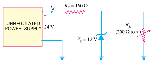
Q8. Fig. 3 shows the zener regulator. Calculate
(i) current through the series resistance
(ii) minimum and maximum load currents and
(iii) minimum and maximum zener currents.
Fig.3
Q9.A zener regulator has VZ = 15V. The input voltage may vary from 22 V to 40 V and load current from 20 mA to 100 mA. To hold load voltage constant under all conditions, what should be the value of series resistance?
Solution.
In order that Zener regulator may hold the output voltage constant under all operating conditions, it must operate in the breakdown region. In other words, there must be Zener current for all input voltages and load currents. The worst-case occurs when the input voltage is minimum and load current is maximum because then Zener current drops to a minimum.
Q10. Determine the minimum acceptable value of RS for the zener voltage regulator circuit shown in Fig. 4.
The zener specifications are :
VZ = 3.3V ; IZ (min) = 3 mA ; IZ (max) = 100 mA
Fig.4
Solution. When load RL goes open (i.e. RL→ ∞), the entire line current IS will flow through the zener and the value of RS should be such to prevent line current IS from exceeding IZ (max) if the load opens.
Q11. Determine the maximum allowable value of RS for the zener voltage regulator circuit shown in Fig. 5.
Fig.5
Solution.
The maximum value of RS is limited by the total current requirements in the circuit.
The value of RS must be such so as to allow IZ (min) to flow through the zener diode when the load is drawing maximum current.
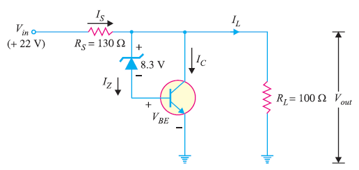
Q12. For the circuit shown in Fig. 6, if VZ = 10V, β = 100 and RL = 1000 Ω , find the load voltage and load current. Assume VBE = 0.5V and the zener operates in the breakdown region.
Q13. A series voltage regulator is required to supply a current of 1A at a constant voltage of 6V. If the supply voltage is 10 V and the zener operates in the breakdown region, design the circuit. Assume β = 50, VBE = 0.5V and minimum zener current = 10 mA.
Solution.
The design steps require the determination of zener breakdown voltage and current limiting resistance RS. Fig. 7 shows the desired circuit of series voltage regulator.
Fig.7
(i) Zener breakdown voltage.
The collector-emitter terminals are in series with the load. Therefore, the load current must pass through the transistor i.e.,
Q14.For the series voltage regulator shown in Fig. 8, calculate (i) output voltage and (ii) zener current.
Fig.8
Q15. In a series transistor voltage regulator (See Fig. 9), the load current varies from 0 – 1A and the unregulated d.c. input varies from 12 – 18V. The 8.5V zener diode requires atleast 1 mA of current to stay in its regulating region (i.e. IZ (min) = 1 mA).
(i) Determine the value of RS to ensure proper circuit operation.
(ii) Determine maximum power dissipation in RS.
(iii) Determine maximum power dissipation in zener doide.
Fig.9
Solution.
(i) The value of RS should be such that it supplies current for the base of transistor Q1 and for the Zener diode to keep it in the regulating region. The worst condition occurs at the minimum input voltage and maximum load current. This means that under the worst conditions, the current through RS must be at least IZ (min) = 1 mA plus maximum base current.
Now 21 mA must be drawn by RS under all conditions of input voltage variations—even when the input voltage falls to 12V which causes the minimum voltage across RS and hence the lowest value of current it will be able to supply.
(iii) Maximum power dissipation in Zener occurs when the current through it is maximum. The Zener current will be maximum when Vin is maximum and load current is minimum (i.e. IL = 0). Now IL = 0 means IE = 0 an hence IB = 0. This, in turn, means that all the current passing through RS will pass through the Zener diode.
Q16. In the series feedback voltage regulator shown in Fig. 10, R1 = 2 kΩ, R2 = 1 kΩ, VZ = 6 V and VBE = 0.7 V. What is the regulated output voltage?
Fig.10
Q17. In the series feedback regulator circuit shown in Fig. 11, R1 = 30 kΩ and R2 = 10 kΩ. What is the closed-loop voltage gain?
Fig.11
Q18. Determine the (i) regulated voltage and (ii) various currents for the shunt regulator shown in Fig. 12.
Fig.12


