Solved Problems on Semiconductor Diode
Last Updated on May 20, 2025 by Sasmita
Semiconductor diodes are fundamental electronic components used extensively in circuits for rectification, signal modulation, voltage regulation, and more. Understanding the practical application of semiconductor diodes through problem-solving is crucial for electronics and electrical engineering students. This article presents a series of solved problems that illustrate how semiconductor diodes operate in various contexts.
Q1. An a.c. voltage of peak value 20 V is connected in series with a silicon diode and load resistance of 500 Ω. If the forward resistance of diode is 10 Ω, find :
(i) peak current through diode (ii) peak output voltage
What will be these values if the diode is assumed to be ideal ?
Solution:
Peak input voltage = 20 V
Forward resistance, rf = 10 Ω
Load resistance, RL= 500 Ω
Potential barrier voltage, V0 = 0.7 V
The diode will conduct during the positive half-cycles of a.c. input voltage only.
The equivalent circuit is shown in Fig.1(ii)
Fig. 1
(i) The peak current through the diode will occur at the instant when the input voltage reaches positive peak i.e. Vin = VF = 20 V.
(ii) Peak output voltage :![]() Ideal Diode Case:
Ideal Diode Case:
Q2. Find the current through the diode in the circuit shown in Fig. 2(i). Assume the diode to be ideal.
Fig. 2
Solution:
We shall use Thevenin’s theorem to find current in the diode. Referring to Fig. 2(i),
Fig. 2 (ii) shows Thevenin’s equivalent circuit. Since the diode is ideal, it has zero resistance
Q3. Calculate the current through 48 Ω resistor in the circuit shown in Fig. 3 (i). Assume the diodes to be of silicon and forward resistance of each diode is 1 Ω.
Fig. 3
Solution:
Diodes D1 and D3 are forward biased while diodes D2 and D4 are reverse biased. We can, therefore, consider the branches containing diodes D2 and D4 as “open”.
Replacing diodes D1 and D3 by their equivalent circuits and making the branches containing diodes D2 and D4 open, we get the circuit shown in Fig. 3 (ii). As we know for a silicon diode, the barrier voltage is 0.7 V.
Q4. Determine the current I in the circuit shown in Fig. 4 (i). Assume the diodes to be of silicon and forward resistance of diodes to be zero.
Fig. 4
Solution:
The conditions of the problem suggest that diode D1 is forward biased and diode D2 is reverse biased. We can, therefore, consider the branch containing diode D2 as open as shown in Fig. 4 (ii).
Further, diode D1 can be replaced by its simplified equivalent circuit.
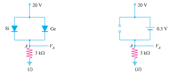
Q5. Find the voltage VA in the circuit shown in Fig. 5 (i). Use simplified model.
Fig. 5
Solution:
It appears that when the applied voltage is switched on, both the diodes will turn “on”. But that is not so. When voltage is applied, germanium diode (V0 = 0.3 V) will turn on first and a level of 0.3V is maintained across the parallel circuit.
The silicon diode never gets the opportunity to have 0.7 V across it and, therefore, remains in open-circuit state as shown in Fig.5(ii).
Q6. Find VQ and ID in the network shown in Fig. 6(i). Use simplified model.
Fig. 6
Solution:
Replace the diodes by their simplified models. The resulting circuit will be as shown in Fig. 6 (ii).
By symmetry, current in each branch is ID so that current in branch CD is 2ID.
Applying Kirchhoff’s voltage law to the closed circuit ABCDA, we have,
Q7. Determine current through each diode in the circuit shown in Fig. 7 (i). Use simplified model. Assume diodes to be similar.
Solution:
The applied voltage forward biases each diode so that they conduct current in the same direction. Fig. 7 (ii) shows the equivalent circuit using simplified model. Referring to Fig. 7 (ii),
Q8. Determine the currents I1, I2 and I3 for the network shown in Fig. 8(i). Use simplified model for the diodes.
Solution:
As we can see in Fig. 8 (i) both diodes D1 and D2 are forward biased. Using simplified model for the diodes, the circuit shown in Fig. 8(i) becomes the one shown in Fig. 8 (ii).
Applying Kirchhoff’s voltage law to loop ABCDA in Fig. 8 (ii), we have,
Q9. Determine if the diode (ideal) in Fig. 9 (i) is forward biased or reverse biased.
Fig. 9
Solution:
Let us assume that diode in Fig.9 (i) is OFF i.e. it is reverse biased.
The circuit then becomes as shown in Fig. 9(ii). Referring to Fig. 9 (ii), we have,
Now V1 – V2 = 2V is enough voltage to make the diode forward biased. Therefore, our initial assumption was wrong, and diode is forward biased.
Q10. Determine the state of diode for the circuit shown in Fig. 10 (i) and find ID and VD . Assume simplified model for the diode.
Fig. 10
Solution:
Let us assume that the diode is ON. Therefore, we can replace the diode with a 0.7V battery as shown in Fig. 10 (ii). Referring to Fig.10 (ii), we have,
Since the diode current is negative, the diode must be OFF and the true value of diode current is ID =0 mA. Hence our initial assumption was wrong.
In order to analyse the circuit properly, we should replace the diode in Fig. 10 (i) with an open circuit as shown in Fig.10(iii).
Fig.10 (iii)
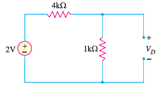
The voltage VD across the diode is :
We know that 0.7V is required to turn ON the diode. Since VD is only 0.4V, the answer confirms that the diode is OFF.


