Solved Problems on Single Stage Transistor Amplifiers
Last Updated on January 9, 2020 by Sasmita
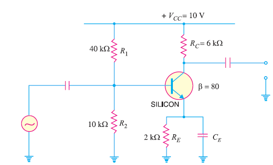
Q1 : Select a suitable value for the emitter bypass capacitor in Fig. 1 if the amplifier is to operate over a frequency range from 2 kHz to 10 kHz.
Fig. 1
Solution :
An amplifier usually handles more than one frequency. Therefore, the value of CE is so selected that it provides adequate bypassing for the lowest of all the frequencies. Then it will also be a good bypass ( XC ∝ 1/f ) for all the higher frequencies.
Suppose the minimum frequency to be handled by CE is fmin. Then CE is considered a good bypass if at fmin,
Q2 :For the transistor amplifier shown in Fig. 2, R1 = 10 kΩ, R2= 5 kΩ, RC = 1 kΩ, RE = 2 kΩ and RL= 1 kΩ.
(i) Draw d.c. load line (ii) Determine the operating point (iii) Draw a.c. load line.
Assume VBE = 0.7 V.
Fig. 2
Solution :
(i) d.c. load line :
To draw d.c. load line, we require two end points i.e., maximum VCE point and maximum IC point.
Maximum VCE = VCC = 15 V
 This locates the point A (OA = 5 mA) of the d.c. load line. Fig. 3 shows the d.c. load line AB.
Fig. 3
(ii) Operating point Q :
The Voltage across series combination of R1 and R2 is 15 V. Applying voltage divider theorem, voltage across
R2 = 5 V.
The voltage across R2 (= 5 kΩ ) is 5 V i.e. V2 = 5 V.
∴ Operating point Q is 8.55 V, 2.15 mA. This is shown on the d.c. load line.
(iii) a.c. load line :
To draw a.c. load line, we require two end points viz. maximum collector-emitter voltage point and maximum collector current point when signal is applied.
This locates the point D (OD = 19.25mA) on the iC axis. By joining points C and D, a.c. load line CD is constructed as shown in Fig. 4.
Fig. 4
Q3 : In the transistor amplifier shown in Fig. 5, RC = 10 kΩ, RL= 30 kΩ and VCC= 20V. The values R1 and R2 are such so as to fix the operating point at 10V, 1mA. Draw the d.c. and a.c. load lines. Assume RE is negligible.
Fig. 5
Solution :
(i) d.c. load line :
For drawing d.c. load line, two end points such as maximum VCE point and maximum IC point are needed.
Maximum VCE = 20 V. This locates the point B (OB = 20V) of the d.c. load line on the VCE axis.
This locates the point A (OA = 2 mA) on the IC axis. By joining points A and B, the d.c. load line AB is constructed as shown in Fig.6.
Fig. 6
(ii) a.c. load line :
To draw a.c. load line, we require two end points viz maximum collector-emitter voltage point and maximum collector current point when signal is applied.
This locates the point C (OC = 2.33 mA) on the iC axis. By joining points C and D, a.c. load line CD is constructed as shown in the above Fig. 6.
Q4 : In the circuit shown in Fig. 7, find the voltage gain. Given that β = 60 and input resistance Rin = 1 kΩ.
Fig. 7
Solution :
So far as voltage gain of the circuit is concerned, we need only RAC, β and Rin
 Q5 : In the circuit shown in Fig. 8, if RC = 10 kΩ, RL = 10 kΩ, Rin= 2.5 kΩ, β =100, find the output voltage for an input voltage of 1mV r.m.s.
Solution :
Q6 : In a transistor amplifier, when the signal changes by 0.02V, the base current changes by 10 μA and collector current by 1mA. If collector load RC = 5 kΩ and RL= 10 kΩ, find: (i) current gain (ii) input impedance (iii) a.c. load (iv) voltage gain
(v) power gain.
Solution :
(ii) input impedance
(iii) a.c. load
(iv) voltage gain
(v) Power gain
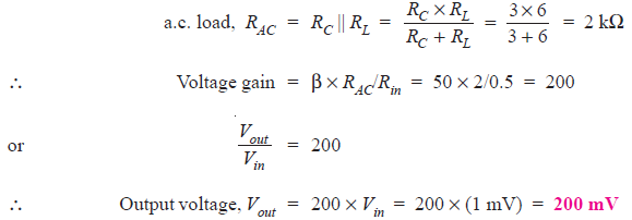
Q7 : In Fig. 9, the transistor has β = 50. Find the output voltage if input resistance Rin= 0.5 kΩ.
Fig. 9
Solution :
β = 50, Rin = 0.5 kΩ
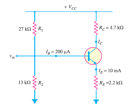
Q8 : Determine the ac emitter resistance for the transistor circuit shown in Fig. 10.
Solution :
Q9 : For the amplifier circuit shown in Fig. 11, find the voltage gain of the amplifier with (i) CE connected in the circuit (ii) CE removed from the circuit.
Fig. 11
Solution :
(i) With CE connected :
(ii) Without CE :
Q10 : For the circuit shown in Fig. 12, find (i) a.c. emitter resistance (ii) voltage gain (iii) d.c. voltage across both capacitors.
Fig. 12
Solution :
(i) In order to find a.c. emitter resistance re′ , we shall first find D.C. emitter current IE . To find IE, we proceed as under:
(ii)
(iii) The d.c. voltage across input capacitor is equal to the d.c. voltage at the base of the transistor which is V2 = 1V. Therefore, d.c. voltage across Cin is 1V.
Similarly, d.c. voltage across CE = d.c voltage at the emitter = VE = 0.3V.
Q11 : For the circuit shown in Fig. 13, find (i) the d.c. bias levels (ii) d.c. voltages across the capacitors (iii) a.c. emitter resistance (iv) voltage gain and (v) state of the transistor.
Fig. 13
Solution :
(i) D.C. bias levels :
The d.c. bias levels mean various d.c. currents and d.c. voltages.
Therefore, all d.c. bias levels stand calculated.
(ii) d.c. voltages across the capacitors
(iii) a.c. emitter resistance
(v) state of the transistor
As calculated above, VC = 10.4V and VE = 2.3V. Since VC > VE, the transistor is in active state.
Q12. An amplifier has a voltage gain of 132 and β = 200. Determine the power gain and output power of the amplifier if the input power is 60 μW.
Solution :
Q13. For the circuit shown in Fig. 14, determine (i) the current gain (ii) the voltage gain and (iii) the power gain. Neglect the a.c. emitter resistance for the transistor.
Fig. 14
Solution :
In most practical circuits, the value of a.c. emitter resistance re′ for the transistor is generally quite small as compared to RE and can be neglected in circuit calculations with reasonable accuracy.
(i)
(ii)
(iii)
Q14. Determine the input impedance of the amplifier circuit shown in Fig. 15.
Fig. 15
Solution :
Q15. An amplifier has an open circuit voltage gain of 1000, an input resistance of 2 kΩ and an output resistance of 1Ω. Determine the input signal voltage required to produce an output signal current of 0.5A in 4Ω resistor connected across the output terminals.
Solution :
Fig. 16 shows the equivalent circuit of the amplifier. Here A0 = 1000.
Fig. 16
Q16. An amplifier has an open circuit voltage gain of 1000, an output resistance of 15Ω and an input resistance of 7kΩ. It is supplied from a signal source of e.m.f. 10mV and internal resistance 3kΩ. The amplifier feeds a load of 35 Ω. Determine (i) the magnitude of output voltage and (ii) power gain.
Solution :
Fig. 17
(i)
(ii)
Q17. An amplifier, when loaded by 2 kΩ resistor, has a voltage gain of 80 and a current gain of 120. Determine the necessary signal voltage and current to give an output voltage of 1V. What is the power gain of the amplifier ?
Solution :
Fig. 18


