Solved Problems on Transistor Biasing
Last Updated on May 21, 2025 by Sasmita
Transistor biasing is a fundamental concept in analog electronics, enabling transistors to operate efficiently in the active region for amplification. Proper biasing ensures a stable operating point (Q-point) despite variations in transistor parameters. This article provides several solved problems on transistor biasing to help students and enthusiasts understand and master the topic.
Q1. An npn silicon transistor has VCC = 6 V and the collector load RC = 2.5 kΩ. Find : (i) The maximum collector current that can be allowed during the application of signal for faithful amplification. (ii) The minimum zero signal collector current required.
Solution:
Fig.1
Collector supply voltage, VCC = 6 V
Collector load, RC = 2.5 kΩ
(i) We know that for faithful amplification, VCE should not be less than 1V for silicon transistor.
∴ Max. voltage allowed across RC = 6 − 1 = 5 V
∴ Max. allowed collector current = 5 V/RC = 5 V/2.5 kΩ = 2 mA
Thus, the maximum collector current allowed during any part of the signal is 2 mA. If the collector current is allowed to rise above this value, VCE will fall below 1 V. Consequently, value of β will fall, resulting in unfaithful amplification.
(ii) During the negative peak of the signal, collector current can at the most be allowed to become zero. As the negative and positive half cycles of the signal are equal, therefore, the change in collector current due to these will also be equal but in opposite direction.
∴ Minimum zero signal collector current required = 2 mA/2 = 1 mA
During the positive peak of the signal [point A in Fig. 1(ii)], iC = 1 + 1 = 2mA
And during the negative peak (point B), iC = 1 − 1 = 0 mA
Q2. A transistor employs a 4 kΩ load and VCC = 13V. What is the maximum input signal if β = 100 ? Given Vknee = 1V and a change of 1V in VBE causes a change of 5mA in collector current.
Solution:
Collector supply voltage, VCC = 13 V
Knee voltage, Vknee = 1 V
Collector load, RC = 4 kΩ
∴ Max. allowed voltage across RC = 13 − 1 = 12 V
∴ Max. allowed collector current, iC =12 V /RC = 12 V/ 4 KΩ = 3 mA
Maximum base current, iB = iC / β = 3 mA / 100 = 30 μA
Now Collector current / Base voltage (signal voltage) = 5 mA/V
∴ Base voltage (signal voltage) = Collector current / (5 mA/V )= 3 mA /( 5 mA/V) = 600 mV
Q3. Fig. 2 (i) shows biasing with base resistor method. (i) Determine the collector current IC and collector-emitter voltage VCE . Neglect small base-emitter voltage. Given that β = 50. (ii) If RB in this circuit is changed to 50 kΩ, find the new operating point.
Solution:
Fig. 2
In the circuit shown in Fig. 2 (i), biasing is provided by a battery VBB (= 2V) in the base circuit which is separate from the battery VCC (= 9V) used in the output circuit.
The same circuit is shown in a simplified way in Fig. 2 (ii). Here, we need show only the supply voltages, + 2V and +9V. It may be noted that negative terminals of the power supplies are grounded to get a complete path of current.
(i) Referring to Fig.2 (ii) and applying Kirchhoff ’s voltage law to the circuit ABEN, we get,
(ii) When RB is made equal to 50 kΩ, then it is easy to see that base current is doubled i.e. IB = 40 μA.
Q4. Fig. 3 (i) shows that a silicon transistor with β = 100 is biased by base resistor method. Draw the d.c. load line and determine the operating point. What is the stability factor ?
Solution:
Fig. 3
Here, VCC = 6 V, RB = 530 kΩ, RC = 2 kΩ
D.C. load line
Referring to Fig. 3 (i), VCE = VCC − ICRC
When IC = 0, VCE = VCC = 6 V. This locates the first point B (OB = 6V) of the load line on collector-emitter voltage axis as shown in Fig. 3 (ii).
When VCE = 0, IC = VCC/RC = 6V/2 kΩ = 3 mA.
This locates the second point A (OA = 3mA) of the load line on the collector current axis. By joining points A and B, d.c. load line AB is constructed as shown in Fig. 3(ii).
Operating point Q
As it is a silicon transistor, therefore, VBE = 0.7V. Referring to Fig. 3(i), it is clear that :
Fig. 3 (ii) shows the operating point Q on the d.c. load line. Its co-ordinates are IC = 1mA and VCE = 4V.
Q5. (i) A germanium transistor is to be operated at zero signal IC = 1mA. If the
collector supply VCC = 12V, what is the value of RB in the base resistor method ? Take β = 100.
(ii) If another transistor of the same batch with β = 50 is used, what will be the new value of zero signal IC for the same RB ?
Solution:
Given, VCC = 12 V, β = 100
As it is a Ge transistor, therefore, VBE = 0.3 V
(i) Zero signal IC = 1 mA
Q6. Calculate the values of three currents in the circuit shown in Fig. 4.
Fig. 4
Solution:
Applying Kirchhoff ‘s voltage law to the base side and taking resistances in kΩ and currents in mA, we have,
Q7. Design base resistor bias circuit for a CE amplifier such that operating point is VCE = 8V and IC = 2 mA. You are supplied with a fixed 15V d.c. supply and a silicon transistor with β = 100. Take base-emitter voltage VBE = 0.6V. Calculate also the value of load resistance that would be employed.
Solution:
Fig. 5 shows CE amplifier using base resistor method of biasing.
Fig. 5
Q8. A base bias circuit in Fig. 6 is subjected to an increase in temperature from 25°C to 75°C. If β = 100 at 25°C and 150 at 75°C, determine the percentage change in Q-point values ( VCE and IC) over this temperature range. Neglect any change in VBE and the effects of any leakage current.
Fig 6
Solution:
At 25°C :
At 75 °C :
Q9. In base bias method, how Q-point is affected by changes in VBE and ICBO.
Solution:
In addition to being affected by change in β, the Q-point is also affected by changes in VBE and ICBO in the base bias method.
(i) Effect of VBE :
The base-emitter-voltage VBE decreases with the increase in temperature (and vice-versa). The expression for IB in base bias method is given by ;
It is clear that decrease in VBE increases IB . This will shift the Q-point (IC = βIB and VCE = VCC – IC RC). The effect of change in VBE is negligible if VCC >> VBE (VCC atleast 10 times greater than VBE).
(ii) Effect of ICBO :
The reverse leakage current ICBO has the effect of decreasing the net base current and thus increasing the base voltage. It is because the flow of ICBO creates a voltage drop across RB that adds to the base voltage as shown in Fig. 7. Therefore, change in ICBO shifts the Q-point of the base bias circuit.
Fig. 7
However, in modern transistors, ICBO is usually less than 100 nA and its effect on the bias is negligible if VBB >> ICBO RB.
Q10. Fig. 8 (i) shows the base resistor transistor circuit. The device (i.e. transistor) has the characteristics shown in Fig. 8 (ii). Determine VCC, RC and RB .
Fig. 8
Solution:
From the d.c load line, VCC = 20V.
Q11. What fault is indicated in (i) Fig. 9 (i) and (ii) Fig. 9 (ii) ?
Fig. 9
Solution:
(i) The obvious fault in Fig. 9(i) is that the base is internally open. It is because 3V at the base and 9V at the collector mean that transistor is in cut-off state.
(ii) The obvious fault in Fig. 9 (ii) is that collector is internally open. The voltage at the base is correct. The voltage of 9V appears at the collector because the ‘open’ prevents collector current.
Q12. For the emitter bias circuit shown in Fig. 10, find IE, IC, VC and VC and VCE for β= 85 and VBE = 0.7V.
Fig. 10
Solution:
Q13. Determine how much the Q-point in Fig. 11 will change over a temperature range where β increases from 85 to 100 and VBE ,decreases from 0.7V to 0.6V.
Fig. 11
Solution:
For β = 85 and VBE = 0.7V
As calculated in the above Question.12, IC = 1.73 mA and VCE = 14.6V.
For β = 100 and VBE = 0.6V
Q14. Fig. 12 shows a silicon transistor biased by collector feedback resistor method. Determine the operating point. Given that β = 100.
Fig. 12
Solution:
VCC = 20V, RB = 100 kΩ, RC = 1kΩ
Since it is a silicon transistor, VBE = 0.7 V.
Assuming IB to be in mA and using the relation,
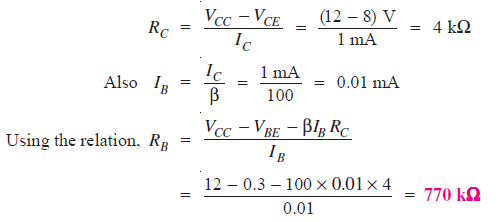
Q15. (i) It is required to set the operating point by biasing with collector feedback resistor at IC = 1mA, VCE = 8V. If β = 100, VCC = 12V, VBE = 0.3V, how will you do it ?
(ii) What will be the new operating point if β = 50, all other circuit values remaining the same ?
Solution:
Given, VCC = 12V, VCE = 8V, IC = 1mA, β = 100, VBE = 0.3V
(i) To obtain the required operating point, we should find the value of RB.
Now, collector load is
(ii) Now β = 50, and other circuit values remain the same.
Q16. It is desired to set the operating point at 2V, 1mA by biasing a silicon transistor with collector feedback resistor RB. If β = 100, find the value of RB.
Solution:
Fig. 13
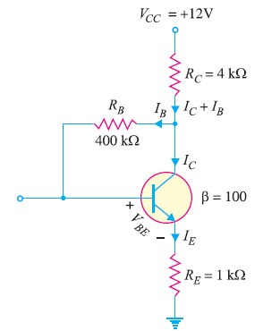
Q17. Find the Q-point values ( IC and VCE) for the collector feedback bias circuit shown in Fig. 14.
Fig. 14
Solution:
Fig. 14 shows the currents in the three resistors (RC, RB and RE) in the circuit. By following the path through VCC , RC, RB, VBE and RE and applying Kirchhoff’s voltage law, we have,
Q18. Find the d.c. bias values for the collector-feedback biasing circuit shown in Fig. 15. How does the circuit maintain a stable Q point against temperature variations ?
Fig.15
Solution:
The collector current is
Stability of Q-point :
We know that β varies directly with temperature and VBE varies inversely with temperature. As the temperature
goes up, β goes up and VBE goes down. The increase in β increases IC (= βIB). The decrease in VBE increases IB which in turn increases IC . As IC tries to increase, the voltage drop across RC (= IC RC ) also tries to increases. This tends to reduce collector voltage VC and, therefore, the voltage across RB. The reduced voltage across RB reduces IB and offsets the attempted increase in IC and attempted decrease in VC . The result is that the collector feedback circuit maintains a stable Q-point. The reverse action occurs when the temperature decreases.
Q19. Fig. 16 shows the voltage divider bias method. Draw the d.c. load line and determine the operating point. Assume the transistor to be of silicon.
Fig. 16
Solution:
d.c. load line :
The collector-emitter voltage VCE is given by :
This locates the second point A (OA = 5 mA) of the load line on the collector current axis. By joining points A and B, the d.c. load line AB is constructed as shown in Fig. 17.
Fig. 17
Operating point :
For silicon transistor, VBE = 0.7 V
Fig.17 shows the operating point Q on the load line. Its co-ordinates are IC = 2.15 mA, VCE = 8.55 V.
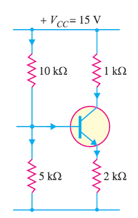
Q20. Calculate the emitter current in the voltage divider circuit shown in Fig. 18. Also find the value of VCE and collector potential VC.
Fig. 18
Solution:
Q21. For the circuit shown in Fig. 19, find the operating point. What is the stability factor of the circuit ? Given that β = 50 and VBE = 0.7V.
Fig. 19
Solution:
Fig. 19 shows the circuit of potential divider bias and Fig. 20 shows it with potential divider circuit replaced by Thevenin’s equivalent circuit.
Fig. 20
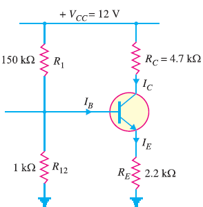
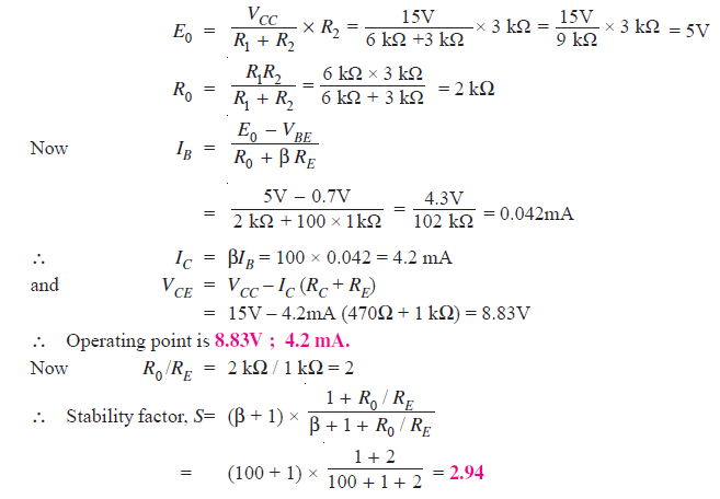
Q22. The circuit shown in Fig. 21 uses silicon transistor having β = 100. Find the operating point and stability factor.
Fig. 21
Solution:
Fig. 21 shows the circuit of potential divider bias and Fig. 22 shows it with potential divider circuit replaced by Thevenin’s equivalent circuit.
Fig. 22
Q23. In the circuit shown in Fig. 23, the operating point is chosen such that IC = 2mA, VCE = 3V. If RC = 2.2 kΩ, VCC = 9V and β = 50, determine the values of R1, R2 and RE. Take VBE = 0.3V and I1 = 10IB .
Fig. 23
Solution:
Given, RC = 2.2 kΩ, VCC = 9V and β = 50, VBE = 0.3V and I1 = 10IB .
As IB is very small as compared to I1, therefore, we can assume with reasonable accuracy that I1 flowing through R1 also flows through R2.
Applying Kirchhoff ‘s voltage law to the collector side of the circuit, we get,
Q24. An npn transistor circuit as shown in Fig. 24 has α = 0.985 and VBE = 0.3V. If VCC =16V, calculate R1 and RC to place Q point at IC = 2mA,VCE = 6 volts.
Fig. 24
Solution:
Given, α = 0.985 , VBE = 0.3V and VCC =16V


