Applications of JK Flip Flop
Last Updated on July 25, 2017 by Sasmita
In our previous article we discussed the J-K flip-flop in detail.
In this article we will study some of the basic applications of the J-K flip-flop. This will include the characteristics of the Toggle (T) flip-flop and the Delay (D) flip-flop connections of J-K flip-flops, which we have already studied in our previous article (Flip-flop conversion) .
Applications of JK Flip Flop
1. Registers
A single flip flop can store a 1 bit word. Thus, by connecting a group of flip-flops, we can increase the storage capacity in terms of number of bits. Such a group of flip-flop is known as a Register.
This means that a n-bit register will consist of n number of flip-flops and it is capable of storing an n-bit word.
Let’s take an example of a 3-bit register . This register can be designed by cascading three D-flip-flops as shown in fig.1 .
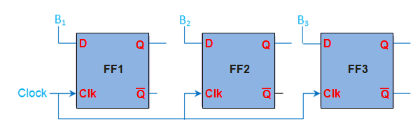
Fig. 1: 3-Bit Register
As shown in fig. 1 , the three bits of information ( B3, B2 and B1 ) can be stored in the three D-flip-flops, thus forminf a 3-bit register. This is also called as 3-bit buffer register .
The binary data stored in the register can be moved within the register from one flip-flop to another upon the application of clock pulses. Such register which allows data transfers is called shift register .
There are various kinds of shift registers viz., serial-in serial-out register, serial-in parallel-out register, parallel-in serial-out register, parallel-in parallel-out register. Further depending on the direction of data movement they can be either left-shift and/or right-shift in nature, as shown by Figure
Depending on the mode of data-shift, there are four mode of operation of a shift register , such as :
- Serial Input Serial Output
- Serial Input Parallel Output
- Parallel Input Serial Output
- Parallel Input Parallel Output
Further depending on the direction of data movement they can be either left-shift and/or right-shift in nature .
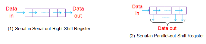
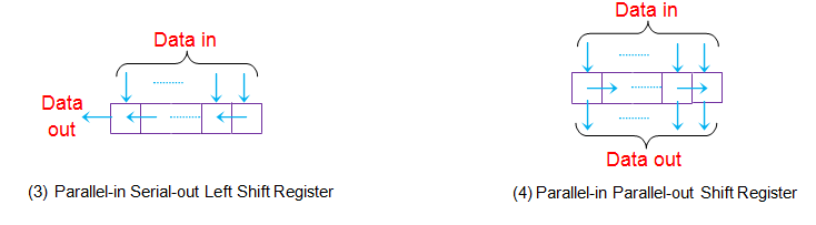
Fig.2 : Different kinds of Shift Registers
Note : (You can have a detailed study of shift registers here .)
2. Counters
Counter is a digital circuit used for a counting pulses or number of events and it is the widest application of flip-flops .
A Counter consists of a series of flip-flops (JK or D or T) arranged in a definite manner . A single flip-flop has two states 0 and 1, which means that it can count upto two.Thus one flip-flop forms a 2-bit (or Modulo 2, MOD 2) counter.
Similarly to count till 8, one needs to connect 3 (= 23) flip-flops in series as shown in Figure 3.
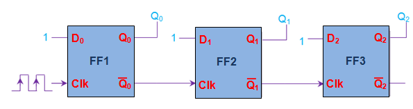
Fig.3 : 3-bit Asynchronous positive edge triggered up-counter
Counters are broadly classified in to two types based on the clock pulse input,as
- Synchronous counter
- Asynchronous counter
These counters can further be classified as positive or negative edge-triggered depending on the connections provided at their clock inputs.
Moreover by slightly modifying the connections between the flip-flops, various other kinds of counters can be designed such as , up-counter, down-counter, up/down counter, ring counter, johnson counter, etc.
3. Event Detectors
An Event detectors is a circuit which is capable of determining the occurrence of a particular event.
These detectors change their state when an event occurs and retain in the same state till that event gets cleared .
Flip-flops are well-known to preserve their state until the appearance of a suitable condition at their inputs, which means they can act as event detectors.
For example, door sensors on a home burglar alarm system use an event detector circuit. Once someone opens the door, the alarm will sound until the system is turned off.
If it were not for the event detection circuit, the alarm would only be on when the door was open. Thus, someone could quickly open the door, enter the house, and close the door. In this situation the alarm would only sound for the brief time that the door was actually open.
4. Data Synchronizers
In a particular combinational circuit all the outputs are expected to change their states at the same instant.
However sometimes due to the varying gate delays, the outputs of the combinational circuit might change their states at different instants of time as shown by the green lines in Figure 4(a) .
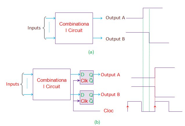
Fig.4 : Data Synchronizing Application of Flip-flop
This would further cause unexpected behavior resulting in wrong outputs.
This can be avoided by using synchronous D flip-flops at the outputs acting as data synchronizers .
In this case, the outputs will be latched by the flip-flops until the clock signal appears. This is shown in fig. 4 (b) .
Thus the outputs can change their states only when the positive edge of the clock triggers the flip-flops which in turn causes the state-change in all the outputs at that particular instant of time.
5. Frequency Divider
Let’s consider a positive edge triggered JK flip-flop whose inputs are tied-together and driven high, as shown in Figure 5.
In this state, the output of JK Flipflop will toggle for each positive-edge of the clock signal (red lines in the figure).
From the waveform it is clear that if the input clock period is Tin, then the time period of output waveform Tout is twice of it.
i.e. Tout = 2 Tin
Thus fout = fin/2
This implies that input frequency is divided by 2.
In other words, after passing through a single flip-flop, the input frequency will be halved.
On the same grounds one can conclude that after passing through the n flip-flops, the input frequency will be divided by 2n which results in
fout = fin/2n
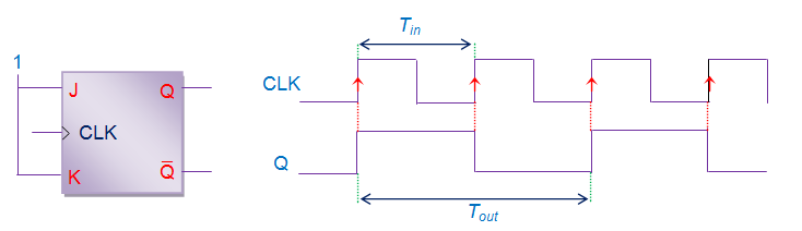
Fig.5