Describe the output Characteristics and transfer characteristics of JFET . Explain different methods of biasing of a JFET
Last Updated on October 8, 2015 by Sasmita
Output Characteristics of JFET
The curve between drain current, ID and drain-source voltage, VDS of a JFET at constant gate-source voltage, VGS is known as output characteristics of JFET.
Drain Characteristic With Shorted-Gate
Fig.1 (i) shows the circuit diagram for determining the drain characteristic with shorted-gate for an n-channel JFET. Fig.1(ii) shows the drain characteristic with shorted-gate.
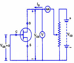
Fig.1(i)

Fig.1 (ii)
when drain-source voltage VDS is zero, there is no attracting potential at the drain, so no current flows inspite of the fact that the channel is fully open. So, drain current ID = 0.
For small applied voltage VDS, the n-type bar acts as a simple semiconductor resistor, and the drain current increases linearly with the increase in VDS, upto the knee point.
This region, to the left of the knee point of the curve is called the channel ohmic region, as in this region the JFET behaves like an ordinary resistor.
With the increase in drain current ID, the ohmic voltage drop between the source and channel region reverse-biases the gate junction.
The reverse-biasing of the gate junction is not uniform throughout. The reverse bias is more at the drain end than at the source end of the channel.
So with the increase in VDS, the conducting portion of the channel begins to constrict more at the drain end. Eventually a voltage VDS is reached at which the channel is pinched off.
The drain current ID no longer increases with the increase in VDS. It approaches a constant saturation value.
The value of voltage VDS at which the channel is pinched off i.e. all the free charges from the channel get removed, and the drain current ID attains a constant value, is called the pinch-off voltage Vp.
From point A (knee point) to the point B (pinch-off point) the drain current ID increases with the increase In voltage VDS following a reverse square law.
The region of the characteristic in which drain current ID remains fairly constant is called the pinch-off region. It is also sometimes called the saturation region or amplifier region.
In this region the JFET operates as a constant current device since drain current (or output current) remains almost constant. It is the normal operating region of the JFET where it is used as an amplifier.
The drain current in the pinch-off region with VGS = 0 is referred to the drain-source saturation current, IDSS).
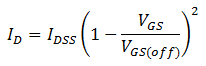
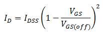
Drain current in the pinch-of region is given by Shockley’s equation:

Where ID = Drain current at given VGS
IDSS = Shorted – gate drain current
VGS = gate-source Voltage
VGS(off) = gate-source cut off voltage
If drain-source voltage, VDS is continuously increased, a stage comes when the gate-channel junction breaks down. At this point current increases very rapidly. and the JFET may be destroyed. This happens because the charge carriers making up the saturation current at the gate channel junction accelerate to a high velocity and produce an avalanche effect.
Drain Characteristics With External Bias
The circuit diagram for determining the drain characteristics with different values of external bias is shown in Fig.2(i). and a family of drain characteristics for different values of gate-source voltage VGS is shown in Fig.2(ii).

Fig.2 (i)

Fig.2 (ii)
It is observed that as the negative gate bias voltage VGS is increased;
(1) The maximum saturation drain current becomes smaller because the conducting channel now becomes narrower.
(2) Pinch-off voltage is reached at a lower value of drain current ID than when VGS = 0.
When an external bias of, say – 1 V is applied between the gate and the source, the gate-channel junctions are reverse-biased even when drain current, ID is zero. Hence the depletion regions are already penetrating the channel to a certain extent when drain-source voltage, VDS is zero.
Due to this reason, a smaller voltage drop along the channel (i.e. smaller than that for VGS = 0) will increase the depletion regions to the point where they pinch-off the current. Consequently, the pinch-off voltage VP is reached at a lower drain current, ID.
(3) Value of drain-source voltage VDS for the avalanche breakdown of the gate junction is reduced.
It is simply due to the fact that gate-source voltage, VGS keeps adding to the reverse bias at the junction produced by current flow.
Transfer Characteristic of JFET
The transfer characteristic for a JFET can be determined experimentally, keeping drain-source voltage, VDS constant and determining drain current, ID for various values of gate-source voltage, VGS.
The circuit diagram is shown in fig.3 (i).
Fig.3 (i)
The curve is plotted between gate-source voltage, VGS and drain current, ID, as shown in fig. 3 (ii).
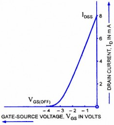
Fig.3 (ii)
It can be observed that:
(i) Drain current decreases with the increase in negative gate-source bias
(ii) Drain current, ID = IDSS when VGS = 0
(iii) Drain current, ID = 0 when VGS = VD
The transfer characteristic can also be derived from the drain characteristic by noting values of drain current, ID corresponding to various values of gate-source voltage, VGS for a constant drain-source voltage and plotting them.
It may be noted that a P-channel JFET operates in the same way and have the similar characteristics as an N-channel JFET except that channel carriers are holes instead of electrons and the polarities of VGS and VDS are reversed.
JFET Biasing
For proper operation of n-channel JFET, gate must be negative w.r.t source. This can be achieved either by inserting a battery in the gate circuit or by a circuit known as biasing circuit. The latter method is preferred because batteries are costly and require frequent replacement.
Bias Battery: In this method, JFET is biased by a bias battery VGG. This battery ensures that gate is always negative w.r.t. source during all parts of the signal.
Biasing Circuit: The biasing circuit uses supply voltage VDD to provide the necessary bias. The two most commonly used methods for biasing are (i) self-bias (ii) potential divider biasing method.
JFET Biasing by Bias Battery
Fig.4 shows the biasing of a n-channel JFET by a bias battery –VGG.
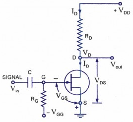
Fig.4
This method is also called gate bias. The battery voltage –VGG ensures that gate–source junction remains reverse biased.
Since the FET has such a high input impedance that no gate current flows, there will be no voltage drop across RG.
Hence, VGS = VGG
We can find the value of drain current ID from the following relation:
The value of VDS is given by:
![]()
Self-Bias for JFET

Fig.5
Fig.5 shows the self-bias method for n-channel JFET.
The resistor RS is the bias resistor. The d.c. component of drain current flowing through RS produces the desired bias voltage.
Voltage across RS, VS = IDRS
Since gate current is negligibly small, the gate terminal is at d.c. ground i.e. VG=0
So, VGS = VG – VS = 0 – IDRS
Or, VGS = – IDRS
Thus bias voltage VGS keeps gate negative w.r.t source.
The drain current ID and drain-source voltage VDS can be calculated from the following relations:
![]()
JFET with Voltage-Divider Bias

Fig.6
Fig.6 shows potential divider method of biasing a JFET.
The resistor R1 and R2 form a voltage divider across drain supply VDD.
The voltage V2 = VG across R2 provides necessary bias.
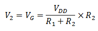
![]()
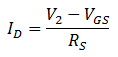
![]()
The circuit is so designed that IDRS is larger than V2 so that VGS is negative. This provides correct bias voltage. We can find the drain current and drain-source voltage as under:
![]()
Although the circuit of voltage divider bias is a bit complex, yet the advantage of this method is that it provides good stability.
Please help me grow this site by following me on Google Plus . You can follow me by clicking the button below.
You Might Like The Following Articles
- What is a Transistor ? Describe the Transistor Action in Detail . Explain the Operation of Transistor as an Amplifier
- Explain the construction and working of a JFET. What is the difference between a JFET and a BJT
- Describe the output Characteristics and transfer characteristics of JFET . Explain different methods of biasing of a JFET
- Explain the construction and working of MOSFET
- Unijunction Transistor
- Discuss the essentials of a transistor Oscillator . Explain the action of tuned collector oscillator , Colpitt’s oscillator and Hartley oscillator