Series Feedback Voltage Regulator
Last Updated on October 1, 2015 by Sasmita
Series Feedback Voltage Regulator
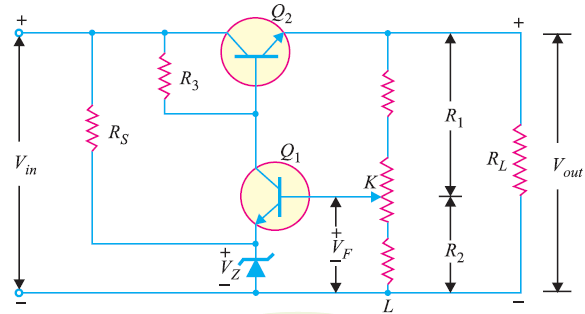
You can see the the circuit diagram of series feedback voltage regulator in the figure below.
So as to keep the output voltage constant (almost constant) despite changes in the load current and line voltage, it employs principles of negative feedback .
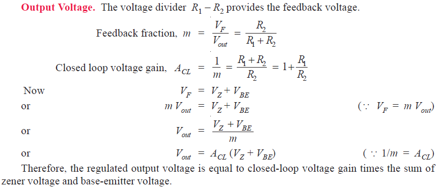
All the load current passes through the transistor Q2 and that’s why it is called a pass transistor. The voltage divider consisting of R1 and R2 is the sample and adjust circuit. The function of the voltage divider is to sample the output voltage and then deliver a negative feedback voltage to the base of Q1. The collector current of Q1 is controlled by the feedback voltage VF.
Operation of Series Feedback Voltage Regulator
As you can see in the circuit diagram, we feed the unregulated d.c. supply to the voltage regulator. The function of the circuit is to maintain constant output voltage despite variations in load or input voltage.
Let’s see how the circuit operates.
Case 1 : Output Voltage Increases
Say, for any reason, the output voltage increases resulting . As a result the voltage across KL (i.e., R2) increases. This in turn means that more VF is fed back to the base of transistor Q1; producing a large collector current of Q1. This causes base voltage of Q2 to decrease as most of this collector current flows through R3. Hence we get less output voltage . In other words the increase in voltage is offset, keeping the output voltage constant.
Case 2 : Output Voltage Decreases
Say, for any reason, the output voltage tries to decreases. As a result the feedback voltage VF also decreases. Hence the current through Q1 and R3 reduces. Which actually means that we get more base voltage at Q2 and more output voltage. Consequently, keeping the output voltage at the original level.
You Might Like The Following Articles
- Regulated DC Power Supply
- DC Voltage Regulator Circuit
- Zener Diode Voltage Regulator
- Transistor Series Voltage Regulator
- Series Feedback Voltage Regulator
- Transistor Shunt Voltage Regulator
- Shunt Feedback Voltage Regulator
- Glow Tube Voltage Regulator
- Series Triode Voltage Regulator
- Series Double Triode Voltage Regulator
- IC Voltage Regulator