Transistor Shunt Voltage Regulator
Last Updated on October 1, 2015 by Sasmita
Transistor Shunt Voltage Regulator
The transistor shunt voltage regulator , regulates voltage by shunting current away from the load to regulate the output voltage.
The circuit diagram of a shunt voltage regulator is shown below.
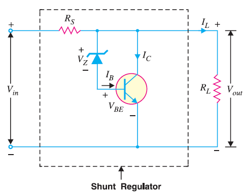
The voltage drop across series resistance depends upon the current supplied to the load RL. The output voltage is equal to the sum of zener voltage (VZ) and transistor base-emitter voltage (VBE)
Vout = VZ + VBE
If the load resistance decreases, the current through base of transistor decreases. As a result, less collector current is shunted. Therefore, the load current becomes larger, thereby maintaining the regulated voltage across the load. Reverse happens should the load resistance increase.
Drawbacks of a Transistor Shunt Voltage Regulator
The following are the drawbacks of a transistor shunt voltage regulator :
- A large portion of the total current through RS flows through transistor rather than to the load.
- There is considerable power loss in RS.
- There are problems of overvoltage protection in this circuit.
- For these reasons, a series voltage regulator is preferred over the shunt voltage regulator.
You Might Like The Following Articles
- Regulated DC Power Supply
- DC Voltage Regulator Circuit
- Zener Diode Voltage Regulator
- Transistor Series Voltage Regulator
- Series Feedback Voltage Regulator
- Transistor Shunt Voltage Regulator
- Shunt Feedback Voltage Regulator
- Glow Tube Voltage Regulator
- Series Triode Voltage Regulator
- Series Double Triode Voltage Regulator
- IC Voltage Regulator